


News
Third generation semiconductor silicon carbide emerging, can be applied to the new wafer cutting process?
With the rapid development of information technology and the growing demand for high-efficiency electronic devices, the third-generation semiconductor materials represented by silicon carbide (SiC) are gradually emerging with their advantages in band gap width, dielectric constant, thermal conductivity and maximum operating temperature. However, silicon carbide as a typical hard and brittle material, its hardness is much higher than traditional silicon materials, Mohs hardness as high as 9.2, second only to the world's hardest diamond, which makes its wafer manufacturing process there are certain challenges.
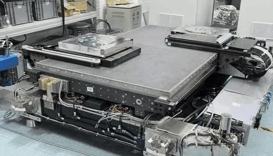
At present, the manufacturing process of silicon carbide wafer is divided into: cutting - grinding - polishing - cleaning, in each processing stage, there are certain requirements for surface damage and roughness, which cutting as the primary process of processing silicon carbide single wafer, its processing quality will greatly affect the subsequent grinding, polishing processing level, and then affect the performance of the chip. In the current industrial production, silicon carbide wafer general multi-wire cutting method, with the continuous progress of technology, water-guided laser cutting, invisible cutting and other new cutting technology has also revealed the edge.
Multi-line cutting technology
Multi-wire cutting technology is the current mainstream wafer cutting technology, compared with the previous saw blade cutting way, to overcome the shortcomings of only cutting one wafer at a time. At present, according to the cutting material, there are mainly two ways of free abrasive wire saw cutting (mortar wire cutting) and diamond wire saw cutting.
01 Free abrasive line saw cutting
Free abrasive line saw cutting machining is a complex process of the interaction of abrasive and workpiece in the cutting line, the cutting mechanism is to use the rapid motion of the line saw to bring abrasive particles in the cutting fluid into the saw joint, driven by the pressure and speed of the cutting line, the free abrasive particles continue to roll in the saw joint, so as to achieve the cutting of materials. When the technology is used to cut silicon carbide ingots, the abrasive particles that play the role of cutting edge materials have a great impact on the cutting effect. Due to the extremely high hardness of silicon carbide, the cutting fluid needs to use diamond micro-powder as the abrasive particles to achieve more efficient cutting purposes, and the mortar, as the carrier of the abrasive particles, plays a stable dispersion and drives the movement of the abrasive particles suspended in it. Therefore, there are certain requirements for its viscosity and fluidity.
02 Consolidated diamond wire saw cutting
Compared with the "three-body processing" of free abrasive wire saw cutting, consolidated diamond wire saw cutting belongs to "two-body processing", and its processing efficiency is several times more than that of free abrasive wire saw cutting, and it has the advantages of narrow slit and small environmental pollution. However, when using this method to cut hard brittle materials such as SiC, there are still shortcomings such as deep damage layer on the surface of the wafer and fast wear of the wire saw. When the diamond line is seriously worn during the cutting process of the wire saw, it will greatly affect the life of the wire saw and the warpage of the wafer. Therefore, the consolidated diamond abrasive wire saw technology is not suitable for the production of ultra-thin large size SiC single wafer.
New laser wafer cutting technology
In recent years, with the continuous development of laser cutting technology, this non-contact cutting technology is also more and more in the production and processing of semiconductor materials, such as the successful application of laser invisible cutting technology for sapphire and silicon wafers, which provides a new solution for silicon carbide (SiC) wafer cutting technology. And derived a variety of laser cutting silicon carbide (SiC) wafer processing methods.
01 Stealth laser cutting technology
Traditional laser cutting is the laser energy in a very short period of time concentrated on the surface of the material, so that the solid sublimation, evaporation of the full cutting processing method, belongs to the laser ablation processing technology. The principle of laser stealth cutting is to use a specific wavelength pulsed laser through the surface of the material to focus inside the material, generate a high energy density in the focus area, forming a multi-photon absorption, so that the required depth of the material to form a modified layer. At the modified layer, because the molecular bonds of the material are broken, when pressure is applied perpendicular to the modified layer of the strip, the ingot is divided into sheets along the crack track.
02 Water guided laser cutting technology
Water-guided laser cutting technology, also known as laser microjet technology, its principle is that when the laser passes through a pressure-modulated water cavity, the laser beam is focused on a very small nozzle, and a very fine high-pressure water column is ejected from the nozzle. Due to the total reflection phenomenon at the interface between water and air, the laser will be confined in a fine water jet, and conducted and focused through the water jet. The laser is then guided by a high-pressure water jet to cut on the surface of the processed material.
Large size single crystal SiC substrate is the mainstream development trend in the future, the current domestic mainstream SiC enterprises have basically achieved comprehensive growth of 6 inches, is developing rapidly in the direction of 8 inches. At present, the most widely used method for slicing silicon carbide ingot is consolidated diamond multi-wire cutting. When cutting large-size wafers, the consolidated diamond wire is prone to wear, which has a certain impact on the cutting quality of wafers. In recent years, a variety of new laser processing technologies such as laser invisible cutting and water-guided laser cutting have provided reliable solutions for the cutting technology of large-size silicon carbide wafers with the advantages of high cutting quality, low cutting damage and high efficiency.
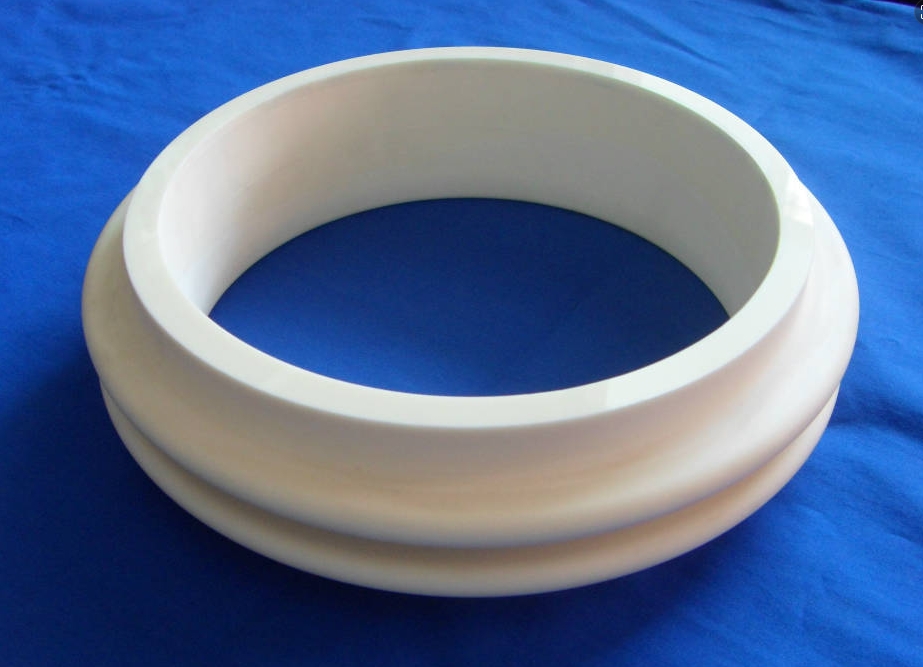
Fountyl Technologies PTE Ltd, is focusing on semiconductor manufacturing industry, main products include: Pin chuck, porous ceramic chuck, ceramic end effector, ceramic square beam, ceramic spindle, welcome to contact and negotiation!