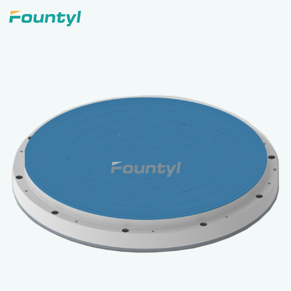
CMP (Chemical Mechanical Polishing) technology is a key process for achieving global uniform and flat wafer surfaces in semiconductor manufacturing
What are the special requirements for the storage and transportation of wafers after they have completed all the processes in the fab? Do special environmental packaging be required?