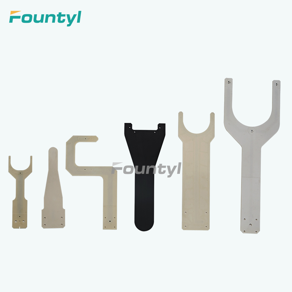
For more than ten years, immersion lithography has been the main exposure technology in semiconductor manufacturing.
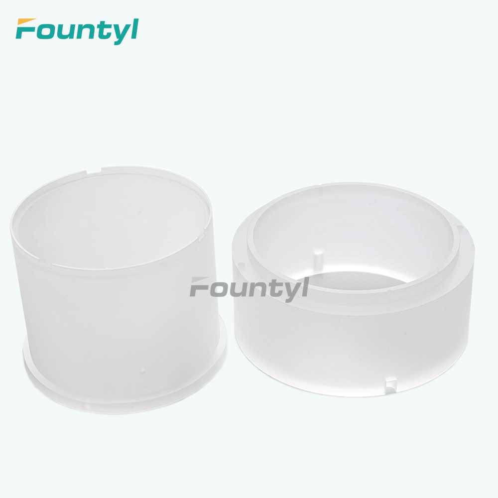
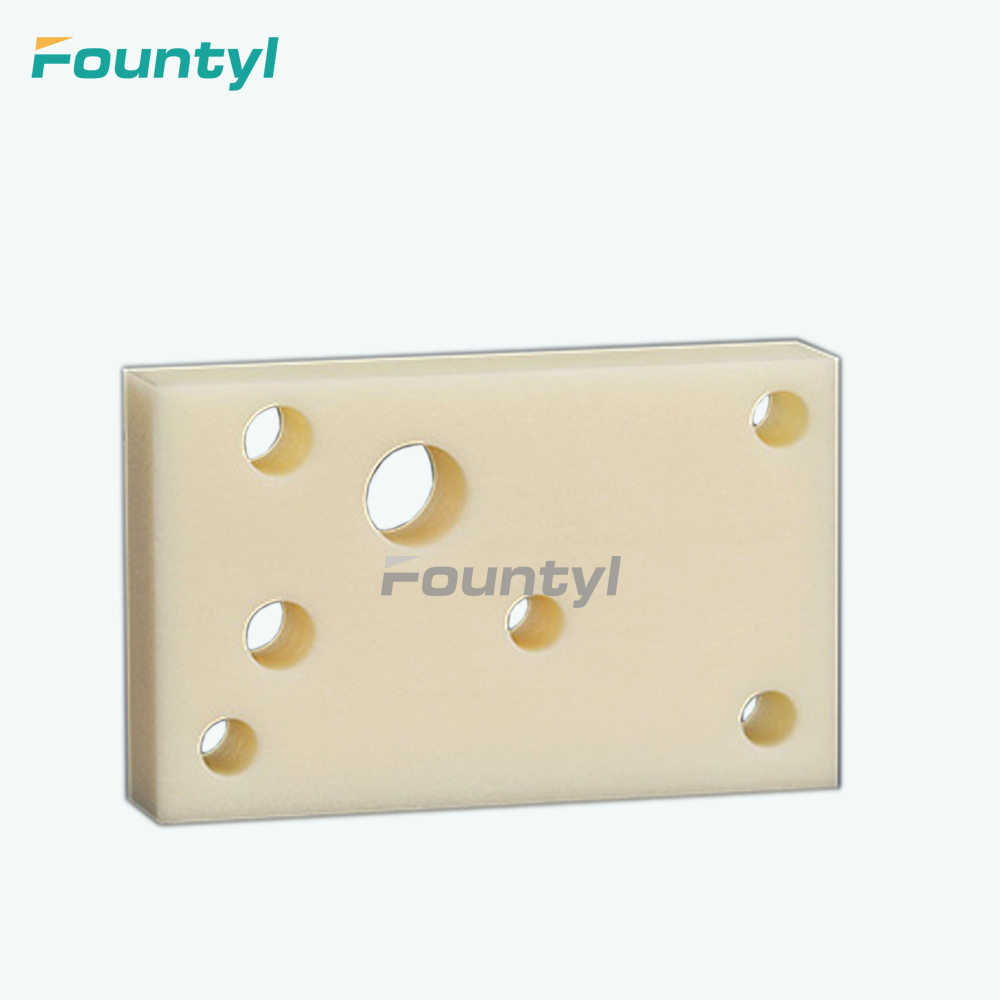
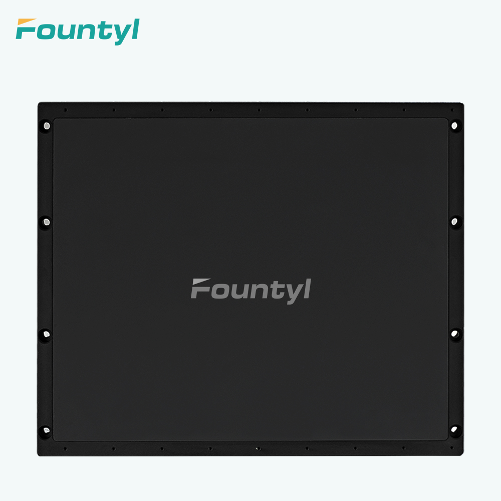
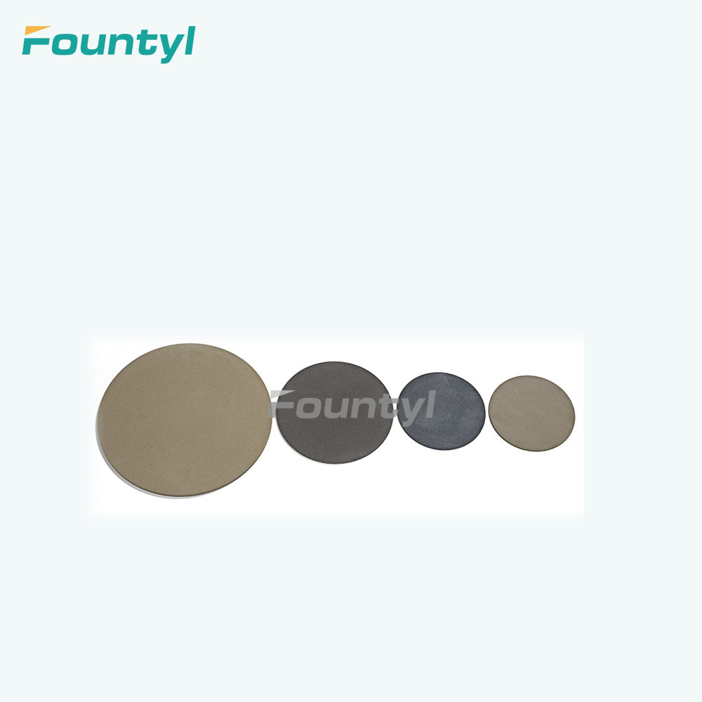
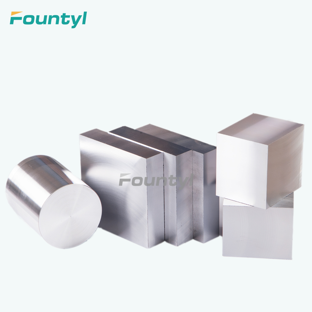
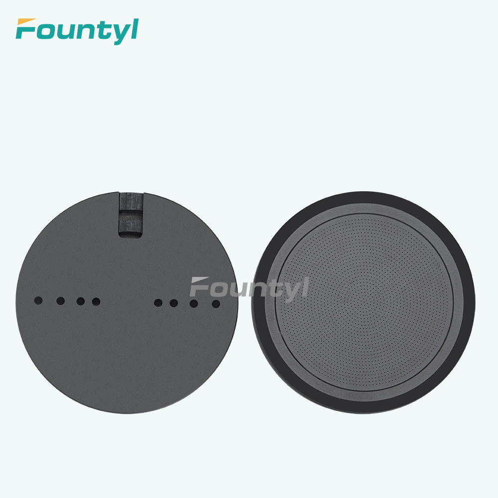
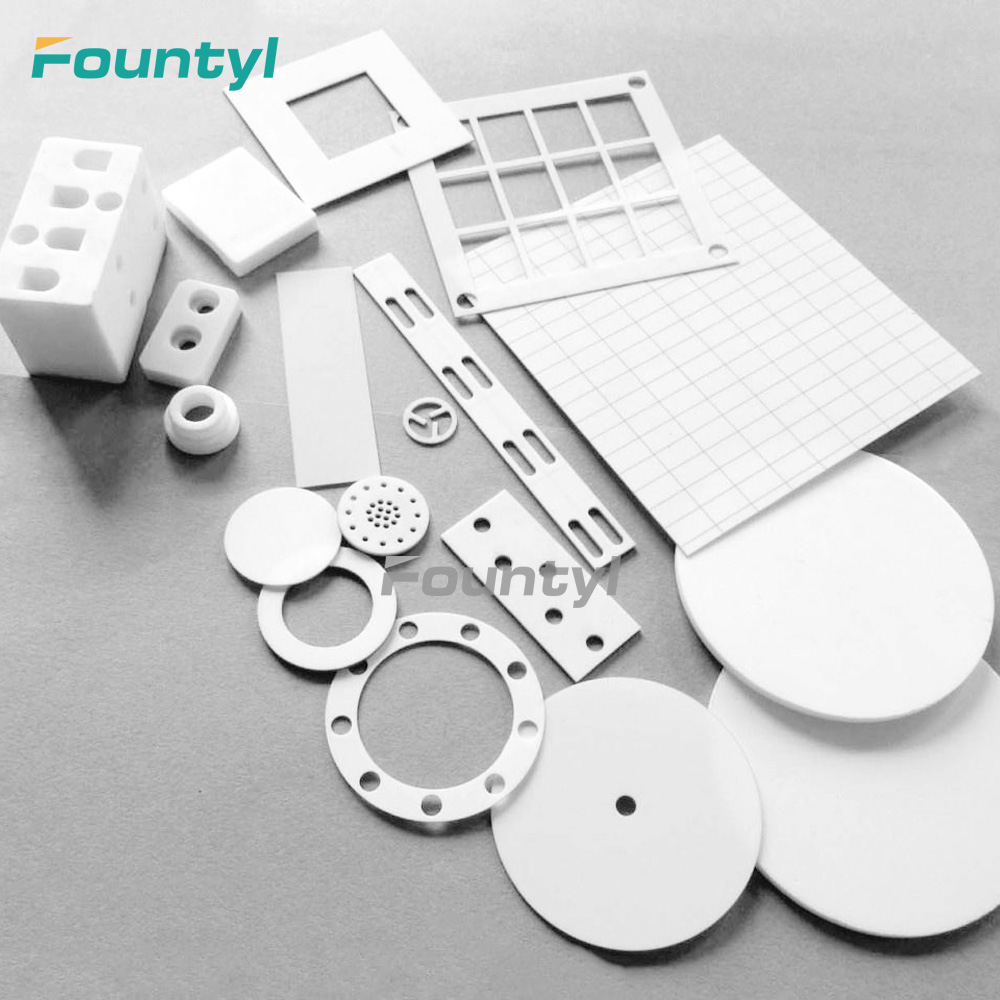
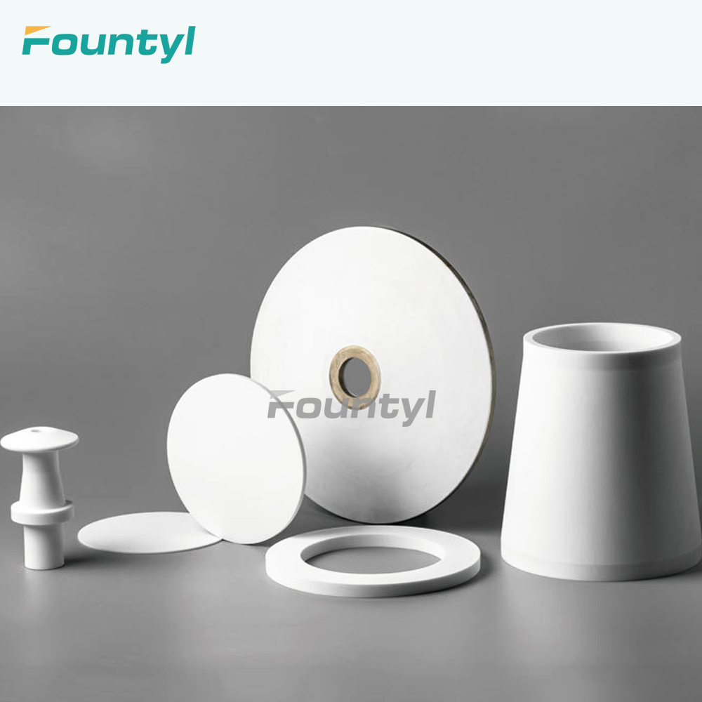
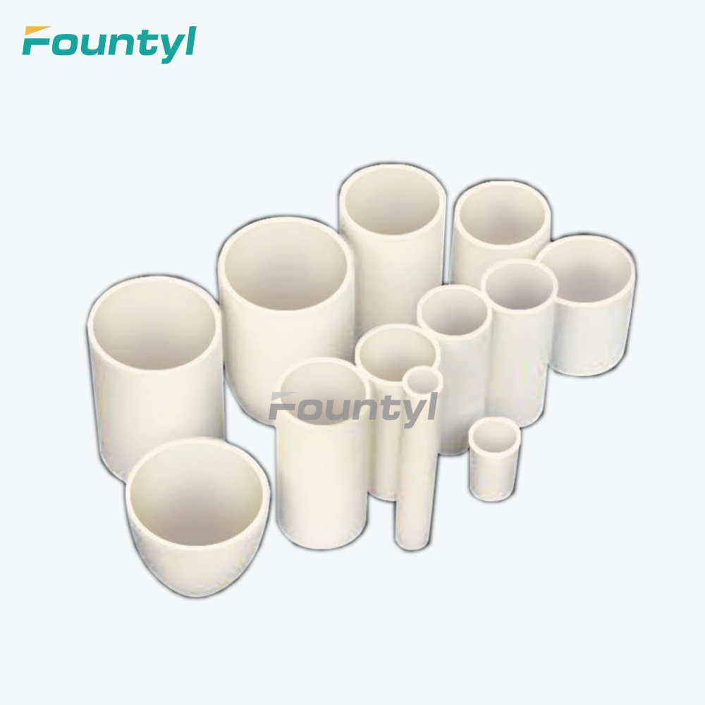
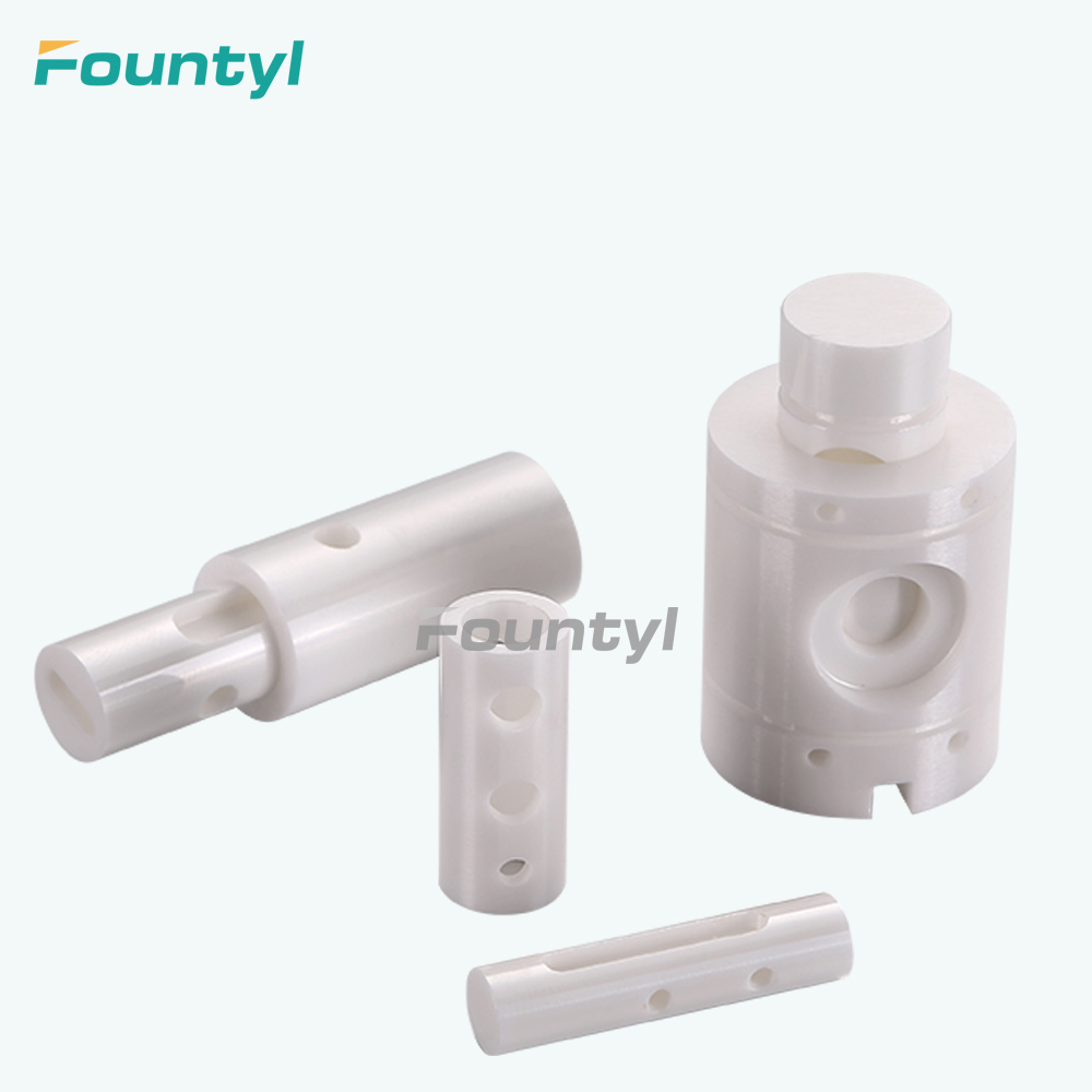
We have developed novel porous ceramics whose pore sizes can be made in the range of less than 1 micron to hundreds of microns. Air is drawn out through tiny pores, and the processed material is p...