

行业博客
History of the world's five largest semiconductor companies
Semiconductor industry chain is too large, semiconductor giant companies are usually through continuous acquisition or merger to enrich their product lines, so as to provide customers with a complete set of solutions.

AMAT (United States Applied Materials) :
1967: Applied Materials was founded
1972: NASDAQ listing
1974: acquisition of Galamar Industries (silicon wafer manufacturing)
1979: Japan branch was established and officially entered Asia
1980: Acquisition of Lintott Engineering (ion implantation)
1984: became the first foreign semiconductor equipment supplier to enter China
1992: surpassed Tokyo Electronics to become the world's largest semiconductor equipment manufacturer
1997: acquired Opal Technologies (IC design high speed metering system); Acquisition of Orbot Instruments (Yield enhancement systems)
1998: Acquisition of Consilium (MES Systems)
1999: acquisition of Obsidian Inc (CMP Technologies); Acquisition of Applied Komatsu Technology (CVD Systems for FPD)
2000: acquisition of Etec Systems (mask pattern production solutions)
2001: Establishment of China headquarters in Shanghai; Acquisition of Schlumberger (electron beam wafer inspection business); Acquisition of Oramir (Wafer Inspection and Control System)
2004: Acquisition of Metron Technology (material management, plant maintenance, etc.) 2005: Acquisition of SCP Global Techbologies' wet Process and wafer cleaning business 2006: Acquisition of Applied Films to enter the solar equipment market
2007: Acquisition of Brooks Software (semiconductor and flat panel display plant management and control software); Acquisition of HCT Shaping Systems SA (wafer system for the production of crystalline silicon substrates for photovoltaic cells); Acquisition of Baccini (Metal coating and inspection systems for crystalline silicon cell manufacturing)
2009: acquisition of Semitool (chip packaging and manufacturing); Set up the world's largest solar technology center in Xi 'an; Closure of thin film solar
2011: Acquisition of Varian Semiconductor (ion implantation, wafer manufacturing)
2013: acquisition of Tokyo Electronics. (2015.4 Cancelled merger)
2019: Acquisition of International Electric. (2021.3 Termination of cooperation)
2021: Opening of Materials Engineering Technology Promotion Center
2022: Acquisition of Picosun (ALD business)
KLA (KLEI) :
1975: KLA establishment
1980: Company listing
1997: acquisition of Tencor (thin film measurement technology)
1998: acquisition of Amray (scanning electron microscopy); Acquisition of Uniphase's Ultirapointe (Silicon Wafer Defect Analysis); Acquisition of Nanopro GmbH (Interferometry); Acquisition of VARS (Production line image management)
1999: acquisition of ACME Systems Inc (volume software analysis)
2000: acquisition of Fab Solutions (process control software); Acquisition of FINLE Technologies (Lithographic Modeling and Data Analysis)
2001: acquisition of Phase Metrics (Data storage inspection certification)
2002: Acquisition of QC Optics (laser inspection system for semiconductor manufacturing) 2004: Acquisition of Candela Instruments (Surface Inspection)
2006: acquisition of Inset (Wafer Monitoring Systems)
2007: acquisition of OnWafer Technologies (Plasma etching) Acquisition of SensArray (real-time temperature measurement technology); Acquisition of Wherma-Wave (real-time Device Services)
2008: acquisition of ICOS Vision Systems (wafer inspection); Acquisition of Vistec Semiconductor (mask measurement)
2009: acquisition of Ambios Technologies (optical profilometers)
2014: acquisition of Luminescent Technologies (luminaires) Acquisition of SPTS Technologies (manufacturing semiconductors, MEMS and other microelectronic devices) 2017: Acquisition of Zeta Technologies (non-contact profiler)
2018: acquisition of Keysight Technologies' Nano Indenter (Mechanical test system) Acquisition of Nanomechanics
2019: acquisition of Filmetrics (film thickness measurement system); Acquisition of Capres A/S (Resistivity Measurement Technology); Acquisition of Orbotech (Semiconductor Inspection)
2021: Acquisition of ECI Technologies (CVS, CPV)
ASML (ASML, Netherlands) :
1984: Royal Philips of the Netherlands and Advanced Semicondutor Materials joint venture established ASML
1986: PAS2500 stepper launched to the market; Established close collaboration with Carl Zeiss
1988: Establishment of the Asian division
1991: Launch of the PAS5500 system
1995: NYSE listing
1999: Acquisition of MaskTools, a business unit of MicroUnity Systems Engineering Inc., to improve the scanning and imaging capabilities of lithography machines Joined Applied Materials to develop EPL (Ion-beam Lithography) project
2000: First TwinSCAN system lithography machine shipped
2001: acquisition of SVG, acquisition of projection mask targeting technology
2007: acquisition of Brion Technologies (Computational lithography integrated circuit) 2008: First YielsStar (250D) shipment
2010: Delivery of the Extreme Ultraviolet (EUV) lithography tool (NXE: 3100), marking the dawn of a new era in lithography
2012: Acquisition of Wijdeven Motion (wafer and optical cover platform manufacturing components), directly impacting nanometer precision
2013: Acquisition of Cymer (manufacturer of lithographic light sources)
2016: acquisition of HMI (electron beam metering Tools); Acquisition of Zeiss SMT (24.9% stake) to strengthen cooperation in semiconductor micrography technology
2019: Acquisition of Mapper (beam electronic lithography machine)
2020: acquisition of Berliner Glas (ceramic and optical module manufacturer)
TEL (Tokyo Electronics) :
1963: Tokyo Electron founded
1965: Agent of Fairchild Semiconductor IC test equipment
1967: Pan-Electronics Co., LTD. Founded, Japan's first imported electronics distributor 1968: TEL-Thermco Engineering
1973: Agency agreement signed with computervision to import CAD/CAM systems
1975: Withdrawal from production and export of consumer electronics
1978: Established the first IC test center in Japan
1980: Listed in Tokyo
1981: TEL-GenRad was established to expand the field of test equipment
1982: TEL-Varian was established and began to develop ion implantation equipment
1995: Acquired Tokyo Electron FE Korea to form Tokyo Electron Korea
2000: Acquired Supercritical System (Wafer cleaning equipment)
2001: Acquisition of Timbre Technologies (semiconductor measurement software)
2006: acquisition of Epion (gas ion beam)
2009: Entry into the photovoltaic equipment market
2012: Acquisition of NEXX Systems (WLP and 3D packaging equipment); Acquisition of FSI International (Cleaning and Surface treatment); Acquisition of Magnetic Solutions (Magnetic Materials and Solutions); Acquisition of Swiss Oerlikon Solar (photovoltaic panel production equipment)
2013: Signed a merger agreement with AMAT (terminated in 2015)
2019: Established cooperation with Bridg
2020: TEL Manufacturing and Engineering of America is established
2022: The listing is transferred to the Prime Market of Tokyo Securities Exchange
LAM (Pan-Forest Semiconductor) :
1980: Company establishment
1991: Wholly-owned subsidiary Pan-Forest Technology Center established in Tokyo
1993: Process research and development Center opened in Japan
1997: Acquisition of Ontrak System (CMP equipment)
2006: Acquisition of Bullen Semiconductor (High purity silicon components and components)
2008: Acquisition of SEZ AG (Wafer cleaning and dry engraving equipment)
2009: Establishment of silfex Corporation (Semiconductor precision Components)
2011: establishment of Corus (Fanlin Korea)
2012: Merger with Novellus Systems (CVD, PVD, CMP, ECD, etc.)
2015: Announced acquisition of KLA-Tencor. (Failed merger announced in 2016)
2017: Acquisition of Coventor (semiconductor manufacturing and MEMS design)
2021: Establishment of manufacturing plant in Malaysia
2022: Acquisition of SEMSYSCO GmbH (high performance computing, artificial intelligence)
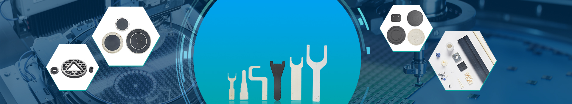
Fountyl Technologies PTE Ltd, is focusing on semiconductor manufacturing industry, main products include: Pin chuck, porous ceramic chuck, ceramic end effector, ceramic square beam, ceramic spindle, welcome to contact and negotiation!