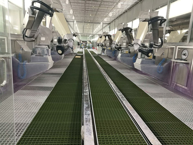
Production Technology
Strict production process and high precision production & testing equipment to ensure the high quality of products.
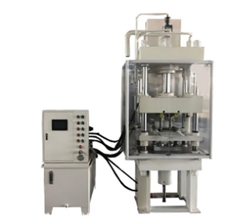
Dry Pressing Process
Dry pressing is one of the most widely used molding process, the main advantages are high molding efficiency, small size deviation of molded products, especially suitable for a variety of small section thickness of ceramic products, such as ceramic valve core, ceramic plate, ceramic ring...etc.
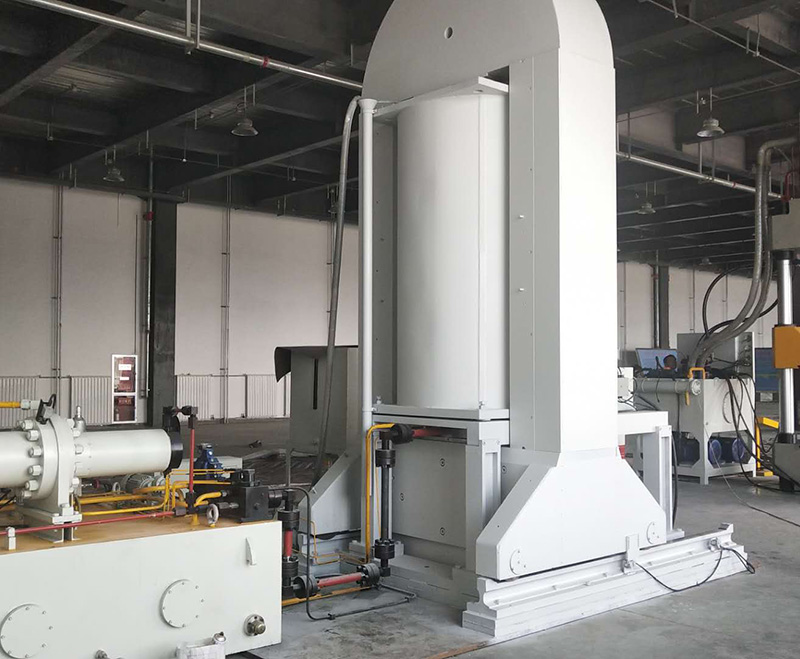
Isostatic Pressing Process And Characteristics
Isostatic Pressing Moulding Has The Following Advantages Over Steel Die Pressing Moulding:
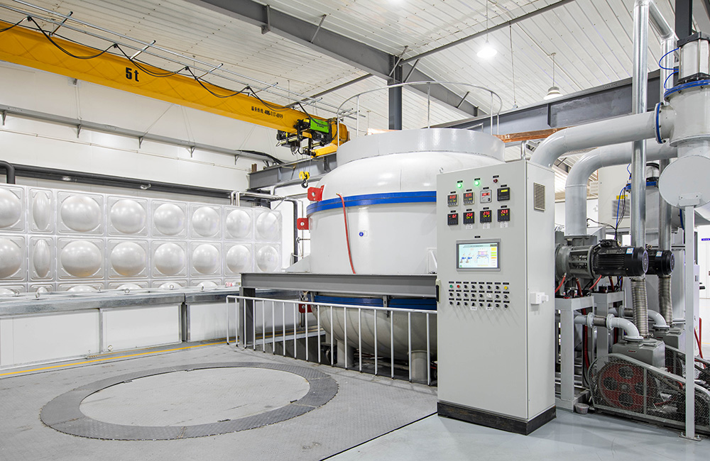
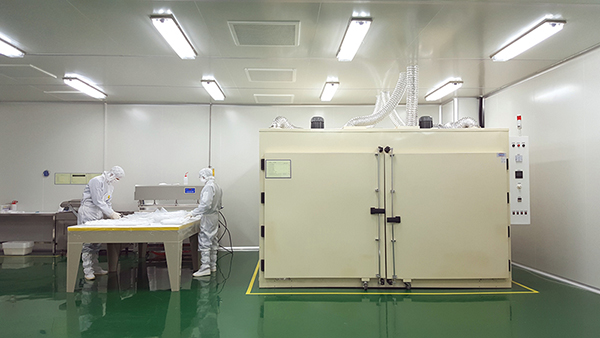
Ceramic Sintering
Ceramic blank is composed of many individual solid particles before sintering, there are a large number of pores in the body, the porosity is generally 35%~60% (that is, the relative density of the blank is 40%~65%), the specific value depends on the characteristics of the powder itself and the molding method and technology used. When the solid blank is heated at high temperature, the particles in the blank transfer, after reaching a certain temperature, the blank shrinks, the grain growth occurs, accompanied by the elimination of pores, and finally the blank becomes a dense polycrystal ceramic material at a temperature below the melting point, this process is called sintering.
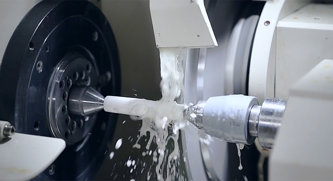
Internal And External Circular Grinding
Inner and outer circular grinding (also known as center grinding) is used to grind the outer circular surface and shoulder of the workpiece. The workpiece is mounted on the center and is rotated by a device called the center driver. Grinding wheels and workpieces are rotated at different speeds by separate motors. The clamping position of the product can be adjusted at an Angle to produce taper. There are five types of external diameter (OD) grinding, internal diameter (ID) grinding, punch grinding, creep feed grinding and centerless grinding.
External Diameter Grinding
External diameter grinding is grinding on the outer surface of an object between the center and the center. The center is an end cell with a point that allows the object to rotate. When the grinding wheel is in contact with the object, the grinding wheel also rotates in the same direction. This effectively means that when contacted, the two surfaces will move in opposite directions, which makes the operation more stability and less blocking.
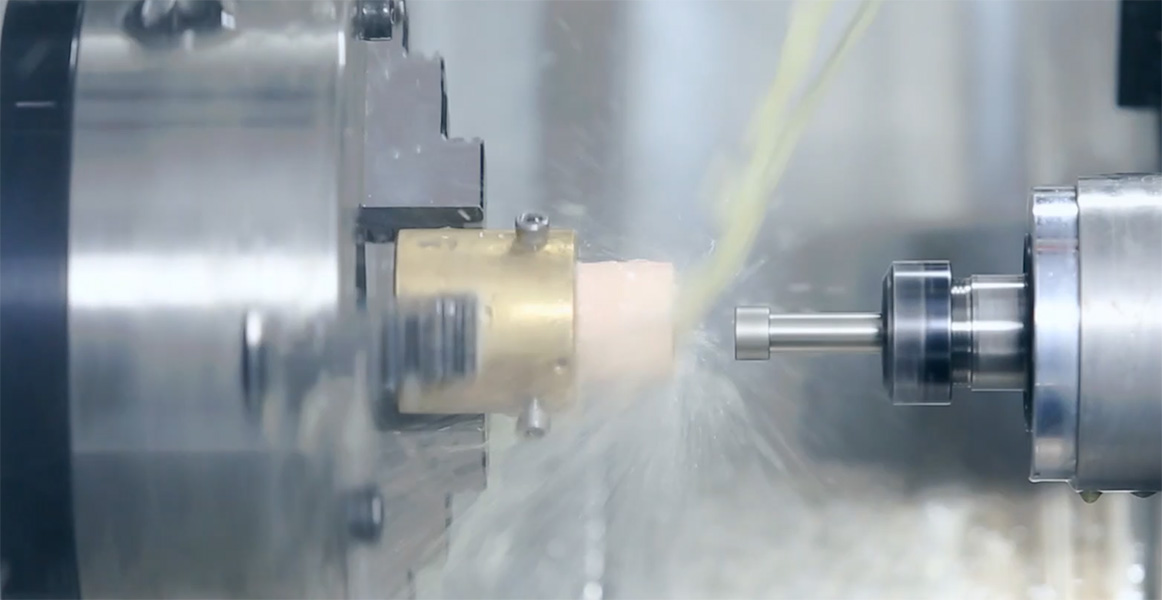
Internal Diameter Grinding
Internal diameter grinding is grinding inside an object. The width of the grinding wheel is always less than the width of the object. The object is held in place by the fixture, which also rotates the object in place. Just like external diameter grinding, the wheel and the object rotate in opposite directions so that the contact direction of the two surfaces where grinding occurs is opposite.
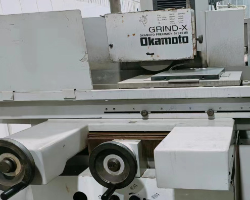
Flat Grinding
Flat grinding is the most common grinding operation. It is a processing technology that uses a rotating grinding wheel to grind the surface of metal or non-metal materials to remove the oxide layer and impurities on the surface of the workpiece, so as to make its surface more refined. A flat grinder is a machine tool designed to provide accurate grinding surfaces, whether critical size or surface finishment. The specific accuracy of the flat grinder depends on its type and use, the diameter is 300mm of disc, the planimetric accuracy can be reach 0.003mm. The maximum processing size of flat grinding: length 1600* width 800mm.
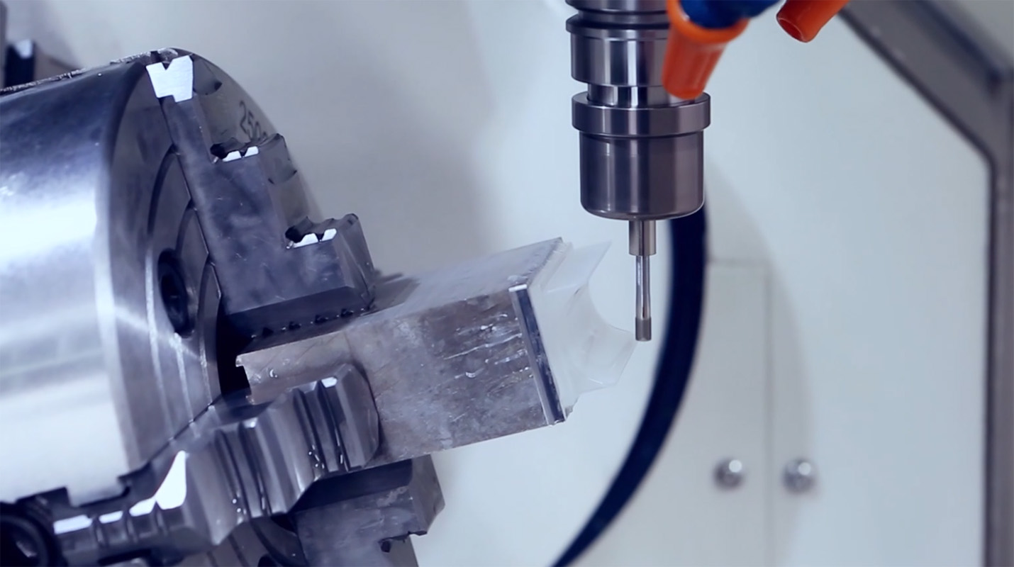
CNC
CNC milling is considered to be one of the most widely used operations in machining. CNC milling is a kind of CNC machine tool with strong processing function, the rapidly developed machining center, flexible machining unit, etc. are produced on the basis of CNC milling machine and CNC boring machine, both are inseparable from the milling method, most industrial milling operations can be completed by 3-axis, 5-axis CNC machine tools. With the advantages of strong adaptability, high processing accuracy, stable processing quality and high production efficiency, this type of path control can process up to 80% of mechanical parts. CNC has a maximum machining size: length 1300* width 800mm.
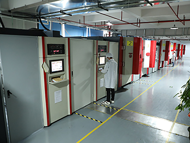
Semiconductor Component Cleaning Process
Wet Cleaning
Wet cleaning is the use of chemical solvents or deionized water to clean the wafer. Wet cleaning can be divided into soaking method and spraying method according to the process method, soaking method is to immerse the wafer into a container tank containing chemical solvent or deionized water. Soaking method is a widely used method, especially for some mature nodes. Spraying, on the other hand, involves spraying a chemical solvent or deionized water onto a rotating wafer to remove impurities. The soaking method can process multiple wafers at the same time, and the spraying method can only process one wafer in one working chamber at the same time. With the development of the process, the requirements of the cleaning process are becoming higher and higher, and the use of spraying method is becoming more and more extensive.
Dry Cleaning
As the name suggests, dry cleaning is not the use of chemical solvents or deionized water, but the use of gas or plasma to clean. With the continuous advancement of technical nodes, the requirements of the cleaning process are becoming higher and higher, the proportion of use is also increasing, and the waste liquid generated by wet cleaning is also a large increase. Compared with wet cleaning, dry cleaning has high investment cost, complex equipment operation and harsher cleaning conditions. However, for the removal of some organic compounds and nitrides, oxides, dry cleaning accuracy is higher, the effect is excellent.
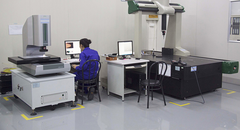
Precision Measurement
We have talents in material research, product development, design, manufacturing and quality management, and have a full set of precision machining and testing equipment: three coordinates, roughness meter, concentricity meter, outer diameter measuring instrument, cylindricity meter of precision testing instruments. Strict production process and high precision production & testing equipment to ensure the high quality of products.
DLC Coating
Wafer carrier/gripper tables are used to contain Si, SiC, GaAs, Gan, and other semiconductor wafers in a variety of semiconductor processes, from detection to lithography, and other high-precision demanding applications, including housing large, thin flexible flat panel displays, MEMS, and biological cells. DLC coatings have many desirable properties, such as durable resistance and high thermal conductivity, to maximize product life, maintain the accuracy, and reduce friction and contamination. The vacuum gripper consists of a rigid body with multiple gripper on the surface of the wafer or panel, and the deviation of the overall and local flatness is measured in nanometers, in this case, the problem with applying a DLC coating on the entire surface of the gripper is that the thermal expansion mismatch can lead to a loss of flatness.
Teflon™ fluoropolymer for semiconductor manufacturing