CMP chemical mechanical polishing equipment principle and the introduction of domestic and foreign equipment manufacturers
Chemical mechanical polishing (CMP) is a technique used to smooth the wafer surface in the process of IC chip manufacturing. By chemical reaction between polishing liquid and wafer surface, an easily processed oxide layer is formed, and then the oxide surface is removed by mechanical action. A uniform flat wafer surface is formed after several alternating chemical and mechanical actions. CMP equipment is a collection of mechanics, fluid mechanics, material chemistry, fine processing, control software and other fields of the most advanced technology in one of the integrated circuit process equipment is more complex and difficult to develop one of the equipment.
Chemical mechanical polishing equipment principle
The CMP device presses the wafer to be polished onto an elastic polishing pad. When polishing, the polishing paste flows continuously between the wafer and the polishing pad. The high-speed reverse operation of the upper and lower plates causes the reaction products on the wafer surface to be continuously peeled off, and the new polishing paste is added, and the reaction products are carried away with the polishing paste. Chemical reactions occur on the newly exposed wafer surface, and the products are stripped off and cycled back and forth, forming a superfine surface under the combined action of substrate, abrasive particles and chemical reactants, as shown in the figure
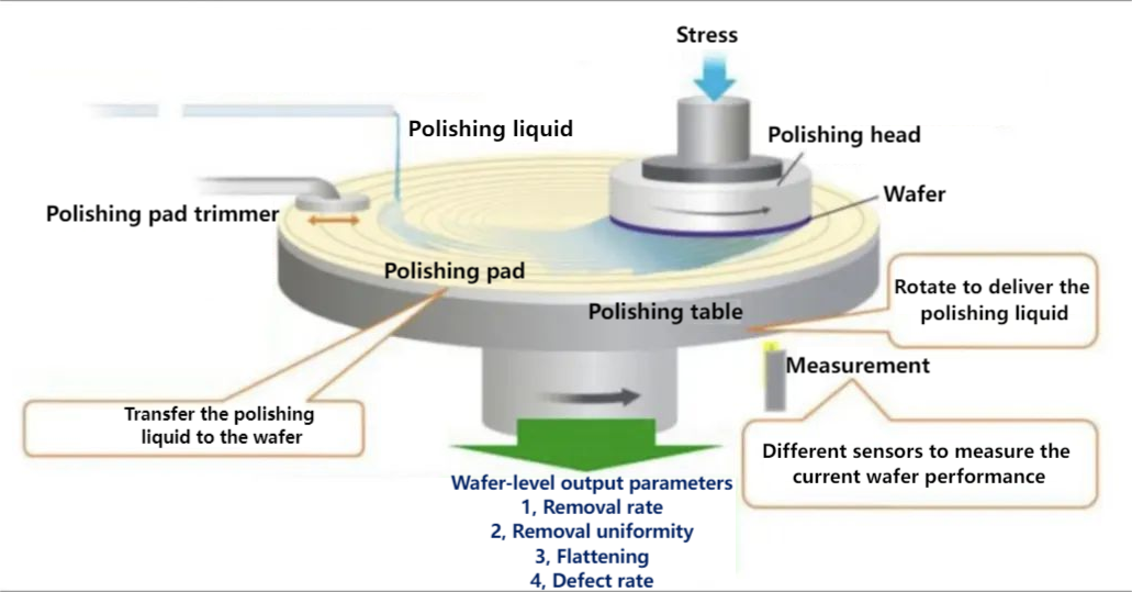
Chemical mechanical polishing equipment development
CMP technology was first proposed by Monsanto in 1965, but was initially used only to obtain high-quality glass surfaces, such as military telescopes. The earliest CMP equipment used on silicon wafers was developed by IBM at its East Fishkill plant in the mid-1980s using Strasbaugh polishes. In 1988, IBM began to use CMP technology in the manufacture of 4M DRAM. By 1990, IBM had sold 4M DRAM using CMP Technology to Micron Technology, and had partnered with Motorola to produce PC components for Apple. After IBM successfully applied CMP to the production of 64M DRAM in 1991, CMP technology has developed rapidly around the world, and since then, various logic circuits and memory have moved to CMP at different scales of development. By 1994, with the mass production of 0.5μm devices and the development of 0.35μm process, the CMP process gradually entered the production line, and the equipment market was initially formed.
Chemical mechanical polishing equipment and consumables market analysis
CMP market is mainly divided into equipment market and consumables market, of which consumables account for nearly 68%, as the main part, equipment is only 32%, so this section will be combined with equipment and consumables for a comprehensive analysis. CMP equipment generally refers to the wafer polishing machine, CMP consumables mainly include polishing paste, polishing pad, cleaning agent, etc., among which, polishing machine, polishing paste, polishing pad is the three key elements of the CMP process, and its performance and matching to a large extent determines the surface flatness level that the chip can achieve after CMP.
CMP equipment market analysis
Although the proportion of the CMP equipment market is much lower than that of consumables, it is the most core element of the CMP process due to its higher technical content. According to the data of China Economic Research Institute, the global CMP equipment market size in 2020 will be $1.767 billion, and $2.783 billion in 2021, with a year-on-year growth of 57.48%. The global market size is expected to be USD 3.076 billion in 2022. CMP equipment is becoming more and more important in the semiconductor Industry, and the U.S. Industry ARC company predicts that the market size of CMP equipment will maintain a compound growth rate of 7.2% from 2020 to 2025 and reach $3.61 billion in 2025. According to the 2020 CMP equipment industry market analysis by Prospective Industry Research Institute, China has jumped to the largest market, accounting for a total of 35% of the global market, of which the mainland market accounted for 25%, and the Taiwan market accounted for 10%; South Korea, the United States, Japan and Europe account for 26%, 13%, 9% and 7% of the global market respectively. According to the research Institute, the United States and Japan lead the way in CMP equipment manufacturing, with Applied Materials (AMAT) of the United States and Ebara Machinery (Ebara) of Japan accounting for 70% and 25% of the global market, respectively. In addition, Peter Wolters of Germany has about 3% of the global market; From the domestic point of view, more than 82% of the mainland market is occupied by foreign enterprises, CMP equipment localization progress is seriously insufficient, only Tianjun Mechanical and electrical, Tianjin Huahai Qingke occupy 12% of the mainland market, 6%, in addition, China Electronics Technology Group Company 45 Institute (referred to as "CLP 45 Institute") has CMP equipment research and development. The latest development of Applied Materials, Ebara Machinery Manufacturing Company, and Pete Walters, the three giants of CMP equipment, Applied Materials is the largest supplier of CMP equipment. In 2003, Applied Materials ended the production of all 8in equipment and focused on 12in CMP equipment. As shown in the figure
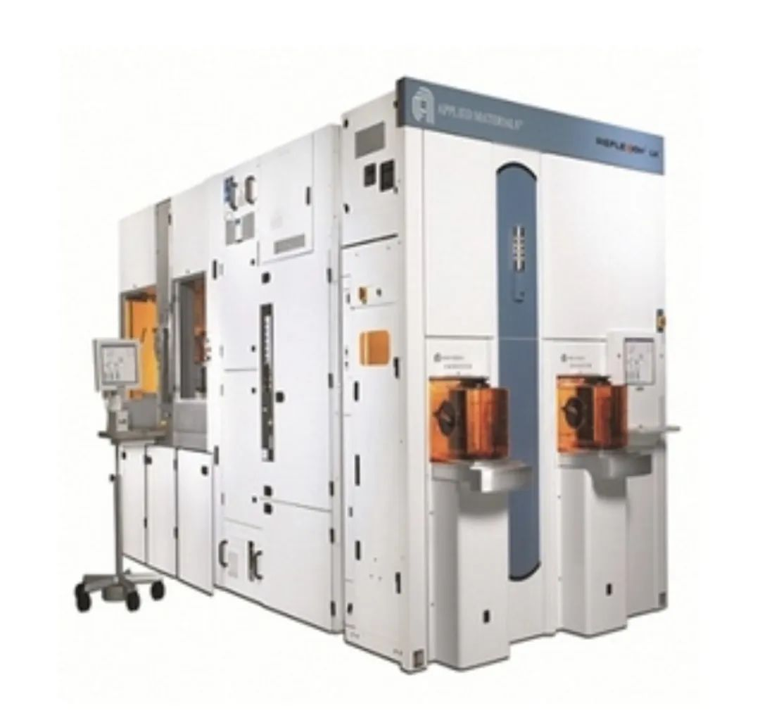
The latest generation of applied materials is ReflexionTM-LK300, part of the classic Mirra family, which provides production-proven, high-performance 150mm and 200mm flattening solutions for silicon, shallow trench isolation (STI), oxide, polysilicon, metallic tungsten and copper inlaying applications. Its high speed flat turntables and multi-zone grinding heads have low pressure for excellent uniformity and efficiency. The MIRRA-equipped integrated CMP aftercleaner Mesa effectively removes slurry, prevents residue formation, and minimizes particles and water marks. For copper Mosaic applications, Applied Materials' CMP equipment is equipped with 200mm Desica cleaning and rinsing technology, which uses Marangoni steam dryers for fast and efficient watermarking free drying. ReflexionTM-LK 300 provides in-line measurement and advanced process control capabilities with a complete endpoint approach, ensuring excellent in-wafer and inter-wafer process control and repeatability for all flattening applications.
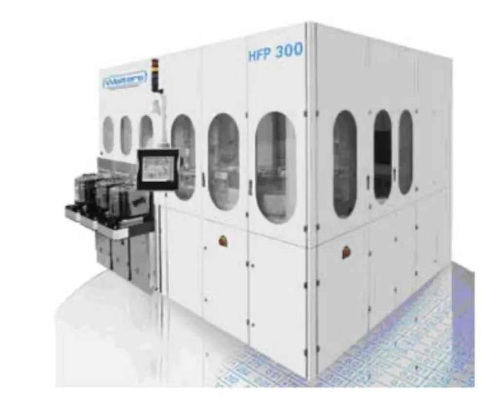
Peter Walters is a well-known semiconductor equipment manufacturer in Europe, has been focusing on the research and development of CMP equipment, and has a unique design and understanding in the field of silicon materials CMP. The CMP equipment produced by Pete Walters mainly includes PM200-Apollo, PM200 GEMINI, PM300-Apollo, HFP200, HFP300, etc., which are rotary CMP equipment, among which the latest generation of PM300-Apollo type is 300mm silicon CMP processing equipment. The function of dry in wet out or dry in dry out can be realized according to different configurations. As shown in Figure 9-4, the HFP300 is the latest 300mm silicon wafer processing equipment developed by Peter Wolters, which improves the production efficiency by 30% compared to the previous generation.
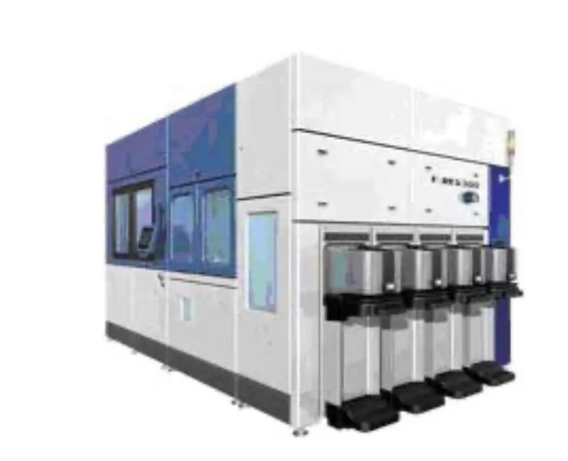
Domestic CMP manufacturers are mainly Tianjun Mechanical and Electrical, Huahai Qingke, CLP 45, in addition, Sheng Mei Semiconductor also launched CMP equipment products in 2019, becoming a new force of domestic CMP equipment. Tianjun Electromechanical, full name is Shanghai Tianjun Electromechanical Equipment Co., LTD., was founded in 2005, is a collection of chemicals, abrasive liquid supply system, wet cleaning equipment research and development, production, sales and service as one of the joint-stock enterprises. Mainly engaged in chemical system CDS, abrasive liquid system SDS, etching wet process WPS, precision ultrasonic cleaning equipment research and development, production, manufacturing.
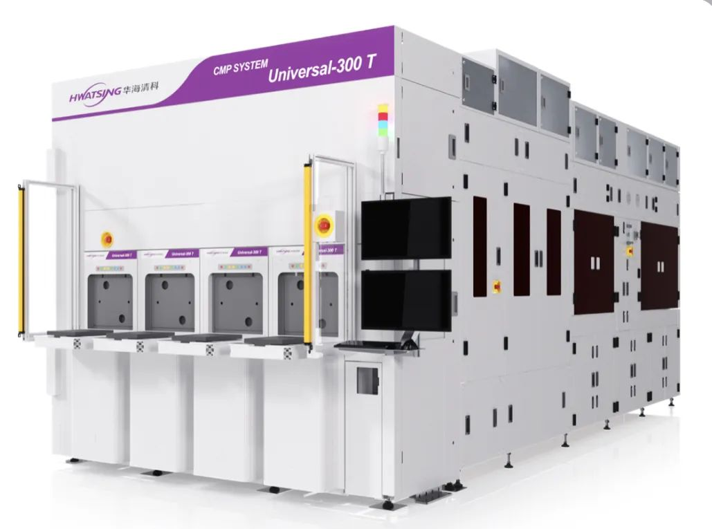
Huahai Qingke's predecessor is the research team established in 2000 under the leadership of Academician Luo Jianbin and Professor Lu Xinchun. In 2012, Academician Luo Jianbin led the research team to successfully develop the first 12in dry in dry out CMP equipment with independent intellectual property rights in China. In March 2013, Tsinghua Holdings and Tianjin Municipality invested in Huahai Qingke. Promote the industrialization process of the scientific and technological achievements. In 2014, Huahai Qingke developed the first 12in dry input and dry output CMP commercial model -Universal-300, as shown in Figure 9-6. The machine entered SMIC Beijing factory in 2015, passed SMIC assessment and achieved sales in 2016.
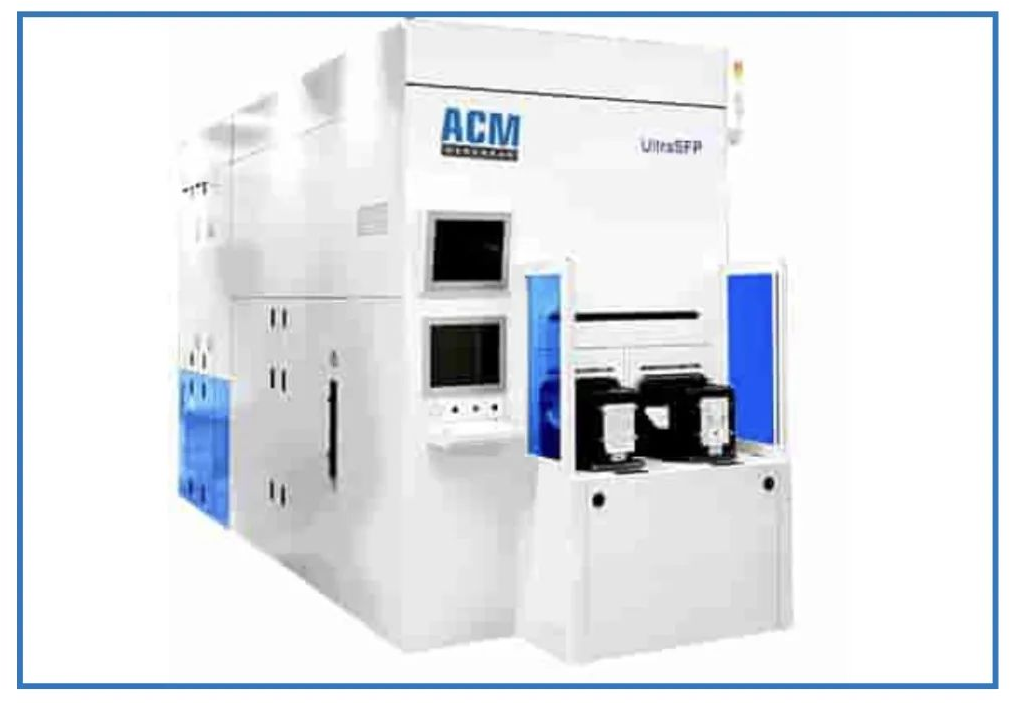
Senmei's CMP equipment is primarily used in the 65 to 45nm copper interconnect process for back-end packages. Senmei Semiconductor has mastered wafer stress-free polishing technology, and prototypes using this technology have been purchased by Intel and LSI Logic. At the "SEMICON China 2019" in Shanghai in March 2019, Shengmei Semiconductor once again released advanced packaging copper throwing equipment, and the newly launched packaging copper throwing equipment is developed for artificial intelligence (AI) chip packaging process. AI chips with more pins require a new three-dimensional packaging process and packaging equipment, and the polishing process requires high cost polishing powder. Shown is the latest UltraSFP ap335 equipment diagram from Semi Semiconductor. For 2.5D packaging process requirements, the UltraSFP ap335 uses a wet electropolishing process, integrating stress free polishing (SFP), chemical mechanical grinding (CMP) and wet etching process (wet etch). It not only reduces the consumption of polishing powder by about 90%, but also recovers the copper in the polishing liquid. Because the chemical liquid of electropolishing can be recycled repeatedly, it can save more than 80% of the cost of supplies.
CMP consumables market analysis
According to the Prospective Industry Research Institute data, the global polishing liquid and polishing pad market size in 2020 will reach 2.01 billion US dollars and 1.32 billion US dollars, respectively. In 2019, the market distribution of various consumables in CMP accounted for a high share of 48.1%, and the polishing pad accounted for 31.6% of the share ranked second, which are the main components of the CMP consumables market.
1) Polishing fluid is one of the key elements of CMP, and its performance directly affects the quality of the polished surface. The composition of polishing paste is mainly composed of three parts: corrosion medium, film forming agent and auxiliary agent, nano abrasive particles. The polishing paste should meet the requirements of fast polishing speed, good polishing uniformity and easy cleaning after polishing. The hardness of abrasive particles should not be too high to ensure that the mechanical damage to the surface of the film is relatively light. In 2019, the global CMP polishing liquid market was $2.01 billion, and the market was mainly monopolized by companies such as Cabot Corporation and Versum in the United States and Fujimi in Japan. Cabot is the world's leading supplier of polishing fluids, with sales revenue of $411 million in 2019 and the highest market share, but its dominance is declining year by year, with its market share falling from about 80% in 2000 to about 35% in 2019. Versum is an established manufacturer of advanced materials and process materials in the United States, with approximately 20% of the global polishing fluid business in 2019. Fujimi is a Japanese company focused on the research and development of abrasive materials, and the sales of CMP polishing liquid reached 14.621 billion yen in 2019, accounting for about 15% of the global share. The main supplier in China is Anji Microelectronics Technology (Shanghai) Co., LTD. (hereinafter referred to as "Anji Technology"), which was established in Pudong New District, Shanghai in 2004, and specializes in a full range of CMP polishing materials and photoresists, with a total revenue of 208 million yuan in 2019.
2) Polishing pad, also known as CMP grinding pad, is mainly composed of polyurethane material containing filling material, used to control the hardness of the wool pad. The protruding part of the surface of the polishing pad directly contacts and fricts with the wafer, and the polishing liquid is evenly sprayed on the surface of the polishing pad to remove the polishing layer, and finally the polishing liquid takes the reaction product out of the polishing pad. The properties of the polishing pad directly affect the surface quality of the wafer and are one of the direct factors related to the flattening effect。
FOUNTYL TECHNOLOGIES PTE. LTD. was located in Singapore, we are focus on the research and development, manufacturing and technical services of precision ceramic parts in the semiconductor field for more than 10 years. our main product are ceramic chuck, ceramic end effector, ceramic plunger and ceramic square beam, including R&D department, QC department, Designing department and sales department.


