


Company News

Singapore porous ceramic chuck table, Southeast Asia precision porous ceramic parts vacuum chuck
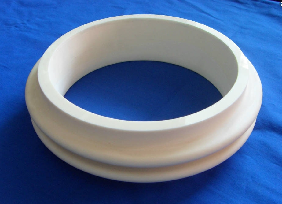
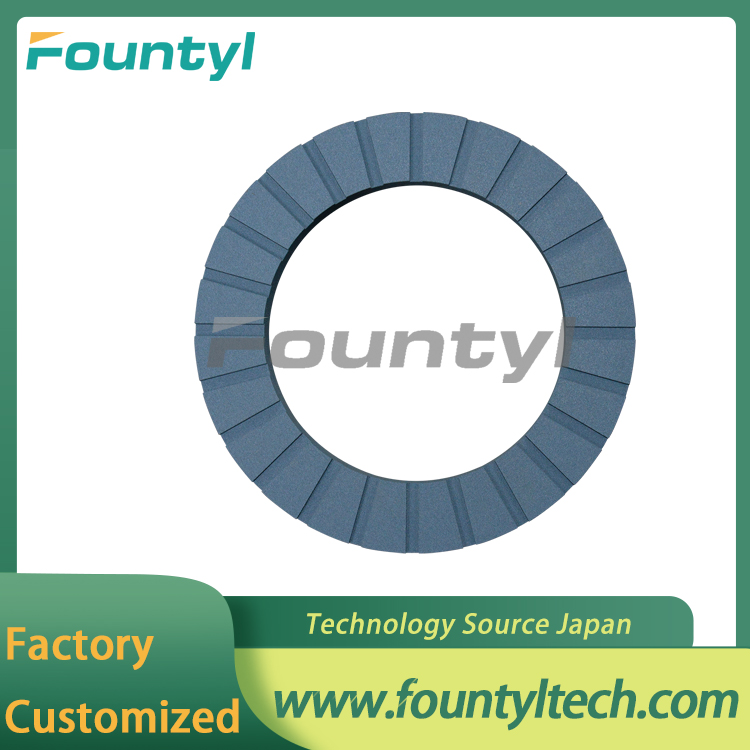
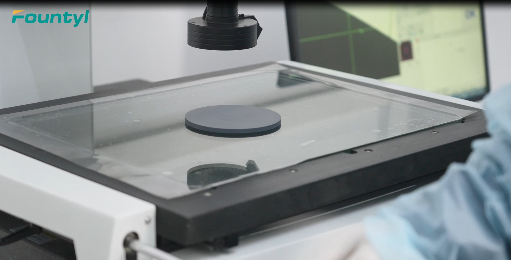
The pore size of the special porous ceramic material is 2 ~ 3 microns, and it is difficult to plug with large vacuum force and partial area adsorption. It can also be used as an air floating platform, which is widely used in semiconductor, panel, laser processing and non-contact linear slider fields. Porous ceramic vacuum chuck maintain transmission by sealing air. The application of the device is limited to the flat, non-porous surface of the working platform. The user is usually the machine operator.
Semiconductor ceramics - custom manufacturing
Fountyl Technologies PTE Ltd is an industry leading ceramic manufacturer of wafer processing equipment technology, and we are constantly optimizing and upgrading the manufacturing process of semiconductor ceramics to achieve better product quality and improve the durability of our products: high aluminum ceramic arms, robotic end effectors, ceramic wafer chucks, wafer handling and machining parts, and custom products. Please consult us directly for detailed dimensions and tolerances
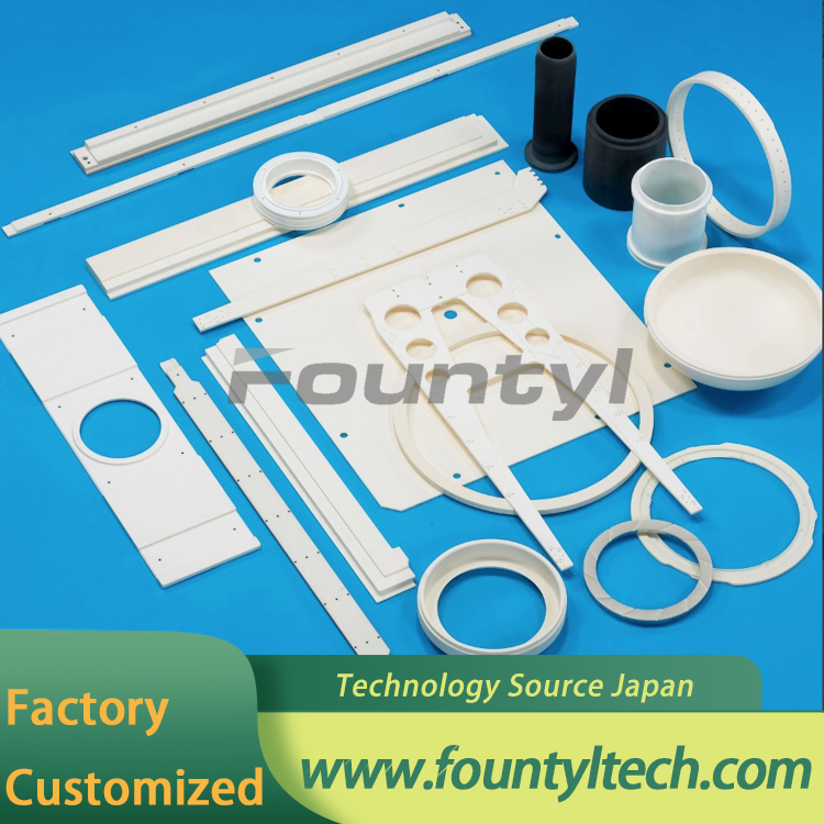
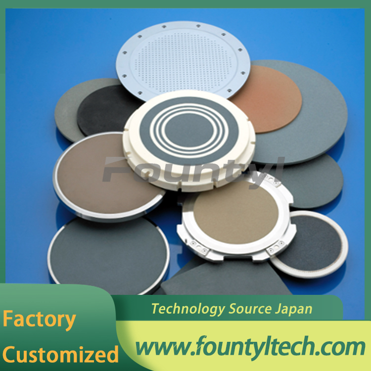
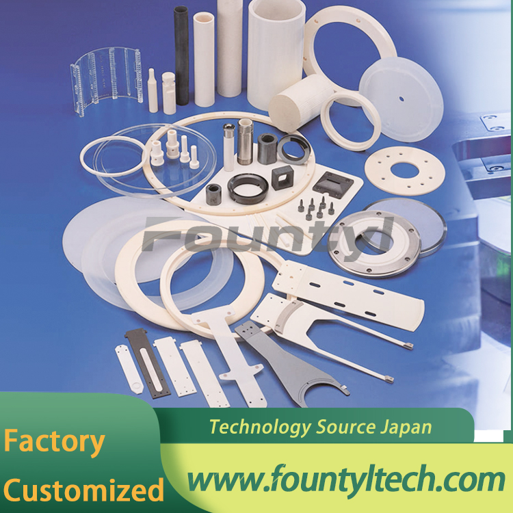
FOUNTYL major product scop of precision ceramic
Management team of Fountyl Technologies PTE Ltd has more than 20 years of semiconductor/panel /MEMS engineering experience, familiar with various materials in the industry application; With reliable materials, stable quality and high-end precision manufacturing technology as the core.
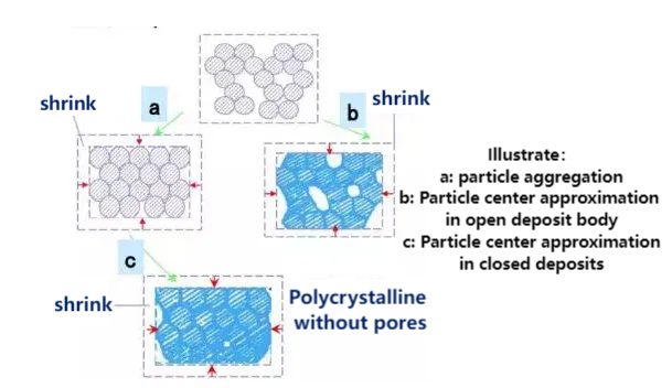
Introduction to microporous ceramics technology
Different from the previous universal cognition of "ceramics", "microporous ceramics" is an industrial material that can be seen everywhere in the industry. When it comes to microporous ceramics, there must be some people who feel very strange to this concept, what is it? What is the difference with our conventional understanding of "ceramics"?
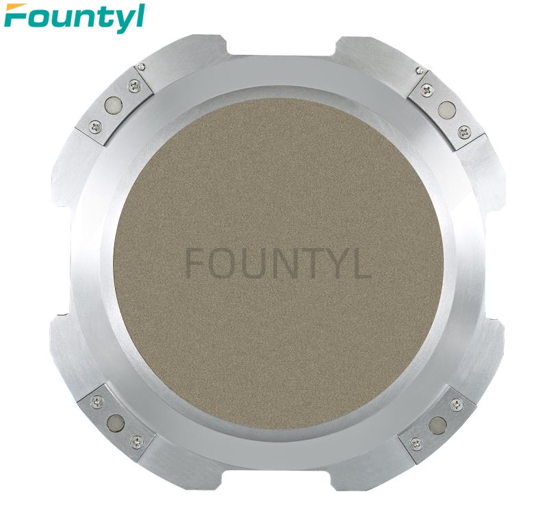
Quality management for ceramic vacuum chuck
FOUNTYL Technologies PTE Ltd is a professional company specializing in the production of porous ceramics, ceramic vacuum chuck, ceramic arms, with many years of industry experience, has a good reputation in the industry, how does Fountyl control the quality of ceramic vacuum chuck?
Why are our porous ceramic vacuum chuck recognized by many engineers and designers?
Why are porous ceramic vacuum chuck recognized by many engineers and designers? What are the characteristics of Fountyl porous ceramic vacuum chuck?
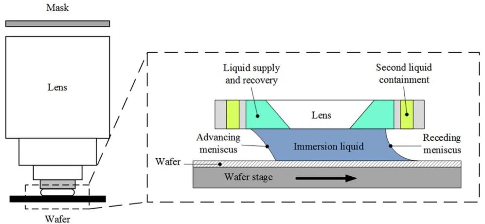
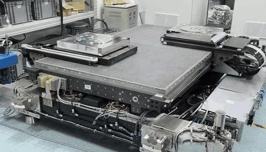
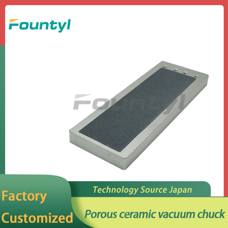
Application of porous ceramic vacuum chuck
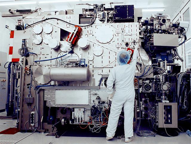
In the semiconductor and optoelectronics industry, very thin wafers are usually placed on advanced ceramic breathable chucks, attached to a vacuum generator, and fixed by vacuum suction. Fountyl Technologies PTE Ltd- special ceramic chuck for silicon wafer waxing, thinning, wax removal, cleaning, cutting processes.
Ceramic bonded with metal
Professional precision ceramics/advanced ceramics/special ceramics manufacturing

Fountyl Singapore will participate in SEMICON Malaysia exhibition in 2024
We are pleased to invite you to our booth at largest congregation of Electronics Supply Chain in SEA @SEMICON SOUTHEAST ASIA 2024.