


News


Semiconductor process and equipment: thin film deposition process and equipment
Thin Film Deposition is the deposition of a layer of nanoscale film on the substrate, and then repeated processes such as etching and polishing, to make a lot of stacked conductive or insulating layers, and each layer has a designed line pattern. In this way, semiconductor components and circuits are integrated into a chip with a complex structure.
Thin film deposition is divided into three of main categories:
◈ Chemical Vapor Deposition (CVD) ◈ Chemical Vapor Deposition (CVD)
◈ Phicial Vapor Deposition (PVD) ◈ Phicial Vapor Deposition
◈ ALD (Atomic Layers Deposition) ALD (Atomic Layers Deposition)
Below we explore thin film deposition technology in depth from these three categories
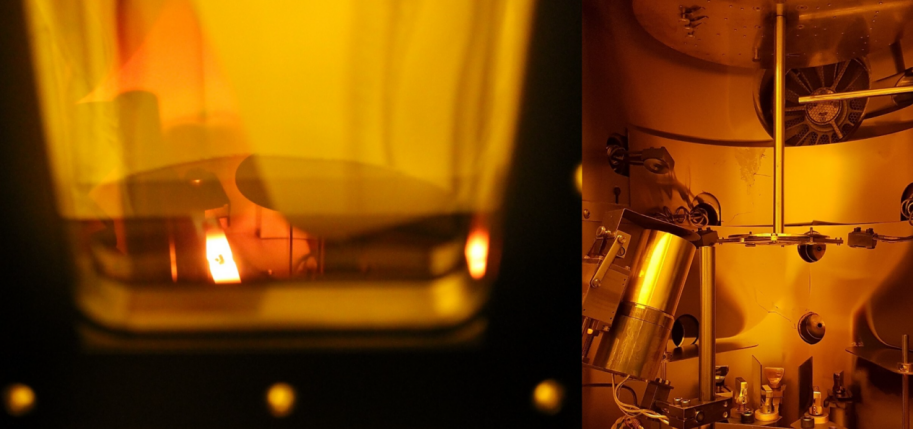
Chemical Vapor Deposition (CVD) process
Chemical vapor deposition (CVD) forms a thin film on the substrate surface by thermal decomposition and/or reaction of gaseous compounds. The film layer materials that can be made by CVD method include carbides, nitrides, borides, oxides, sulfides, selenides, tellurides, and some metal compounds, alloys, etc.
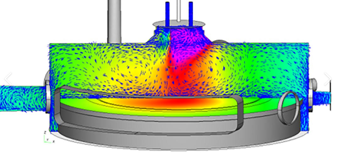
Physical Vapor Deposition (PVD) process
Under vacuum conditions, using physical methods, the surface material of the material source (solid or liquid) is vaporized into gaseous atoms, molecules or partially ionized into ions, and through the low pressure gas (or plasma) process, the film with a special function is deposited on the surface of the substrate technology. Physical vapor deposition can not only deposit metal film, alloy film, but also deposit compounds, ceramics, semiconductors, polymer films and so on.
There are also various processes for physical vapor deposition:
◈ 真空蒸度 Thin Film Vacuum Coating
◈ 溅射镀膜 PVD-Sputtering
◈ 离子镀膜 Ion-Coating
Atomic Layer Deposition (ALD) process
Atomic Layers Deposition (ALD) is a high-precision thin film deposition technology based on chemical vapor deposition (CVD), which deposits material layer by layer on the substrate surface in the form of a single atomic film based on chemical vapor phase.
Different from traditional CVD, in the deposition process of ALD, the reaction precursor is alternately deposited, and the chemical reaction of the new atomic film is directly related to the previous layer, so that only one layer of atoms is deposited in each reaction.
Only one layer of atoms is deposited in each reaction, which has the characteristics of self-restricted growth, so that the film can be conformal and deposited on the substrate without pinholes. Therefore, the film thickness can be precisely controlled by controlling the number of deposition cycles.
ALD can be deposited materials including metals, oxides, carbon (nitrogen, sulfur, silicon) compounds, various semiconductor materials and superconducting materials. With the integration of integrated circuits getting higher and higher, the size is getting smaller and smaller, the high dielectric constant (high k) gate medium gradually replaces the traditional silicon oxide gate, and the aspect ratio is getting larger and larger, which puts higher requirements on the step coverage capability of deposition technology, so ALD has been used more and more as a new deposition process that can meet the above requirements.
Fountyl Technologies PTE Ltd, is focusing on semiconductor manufacturing industry, main products include: Pin chuck, porous ceramic chuck, ceramic end effector, ceramic square beam, ceramic spindle, welcome to contact and negotiation!