


News

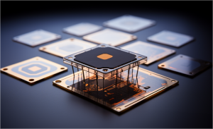
Application of PVD technology in semiconductor devices
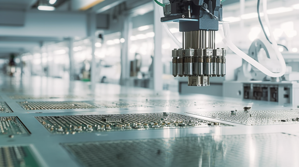
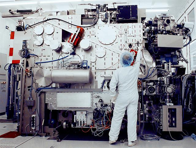
Physical vapor deposition(PVD)involves depositing a thin film on a semiconductor substrate, using physical processes such as sputtering or evaporation. The versatility and controllability of PVD makes it a valuable tool in semiconductor manufacturing to create complex and high-performance devices.
Application of PVD in advanced microelectronics
Thin film transistor (TFTs)
PVD plays a key role in the manufacturing of TFTS, which are essential components of flat panel displays, organic light-emitting diodes (OLeds), and other emerging display technologies. PVD technology has improved the performance of TFT, improved response time, and reduced power consumption, making a significant contribution to the development of display technology.
Interconnection and metallization:
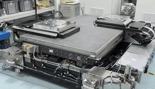
As semiconductor devices become more compact, efficient interconnections become critical. PVD helps create reliable metal interconnects with minimal resistivity, increasing signal speed and device reliability. The case study will clarify the key role of PVD in advanced metallization processes, ensuring optimal equipment performance.
Semiconductor packaging:
PVD plays an important role in the production of protective coatings for semiconductor devices, protecting them from environmental factors and ensuring longevity. We will delve into how PVD can help create a protective layer that improves the durability and reliability of equipment, especially in challenging operating environments.
The implementation of physical vapor deposition (PVD) in logic and memory device manufacturing has revolutionized semiconductor memory technology.
Here are some real-world examples that demonstrate the important role of PVD in the field.
1. High-density memory storage:
In the field of high-density memory storage, PVD technology has played an important role in pushing the boundaries of data storage capabilities. The case study reveals examples of PVD being used to deposit thin films with exceptional precision, enabling the creation of densely packed storage units. This not only maximizes storage capacity, but also increases the speed of data retrieval, thereby increasing the efficiency of storage devices.
2. Logic circuit performance enhancement:
Logic circuits are the backbone of semiconductor devices, and PVD plays a key role in improving their performance. By controlling the deposition process, PVD ensures the creation of high-quality interconnects and metal layers, reducing resistivity and improving signal propagation. The case study highlights how PVD can help manufacture logic circuits with superior speed, reliability, and energy efficiency.
The precision and reliability provided by PVD technology are key factors in the continuous advancement of semiconductor memory technology, pushing the boundaries of what is achievable in terms of storage capacity and processing speed.
PVD for advanced Sensor technology:
The application of physical vapor deposition (PVD) in the development of advanced sensor technology has a profound impact on various fields such as automotive, healthcare and consumer electronics. Here are some illustrative examples that highlight the key role of PVD in this area.
1. Car sensor:
In the automotive industry, sensors are an important part of a variety of applications, including safety systems and engine management. PVD is used to form a thin film on the surface of the sensor, improving sensitivity and response time. Real-world examples demonstrate how PVD can help improve the accuracy of automotive sensors, enabling advancements in driver assistance systems and overall vehicle safety.

2. Medical sensor:
PVD plays an important role in the development of sensors used in healthcare applications such as medical imaging devices and diagnostic tools. Through a precise deposition process, PVD ensures the creation of a sensor coating that improves sensitivity and biocompatibility. The case study demonstrates how PVD can contribute to the production of reliable and accurate healthcare sensors, ultimately improving patient care and diagnostic capabilities.

3. Consumer electronics sensors:
From touch screens to motion sensors, consumer electronics rely on sensors for a variety of functions. PVD technology is used to create a protective and conductive layer on the sensor surface for increased durability and responsiveness. Examples highlight how PVD enhances the reliability of sensors in consumer electronics, contributing to the seamless and efficient operation of devices.
Conclusion:
As semiconductor devices continue to evolve in terms of complexity and functionality, the role of PVD in their manufacturing is becoming increasingly important. This article provides a comprehensive overview of the advanced applications of PVD technology in the semiconductor industry, providing insight into its impact on the creation of cutting-edge electronic devices. The versatility of adopting PVD opens up new possibilities for innovation and ensures that the semiconductor industry remains at the forefront of technological advances.
Fountyl Technologies PTE Ltd, is focusing on semiconductor manufacturing industry, main products include: Pin chuck, porous ceramic chuck, ceramic end effector, ceramic square beam, ceramic spindle, welcome to contact and negotiation!