


News
Common wafer adsorption technology
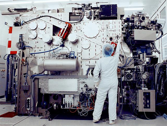
Wafer adsorption technology is a seemingly trivial but crucial link. Whether etched, deposited or lithographed, wafers must be stably and precisely fixed in the right position to ensure efficient chip production.
Several common wafer adsorption methods:
Mechanical vacuum adsorption
Mechanical vacuum adsorption creates a negative pressure environment through a vacuum pump, which is used to draw air from the adsorption area, thereby reducing the pressure and creating a vacuum area between the wafer and the adsorption disc. Seals are usually required to ensure the sealing of the adsorption area and prevent outside air from entering. This creates enough suction to stably adsorb the wafer.
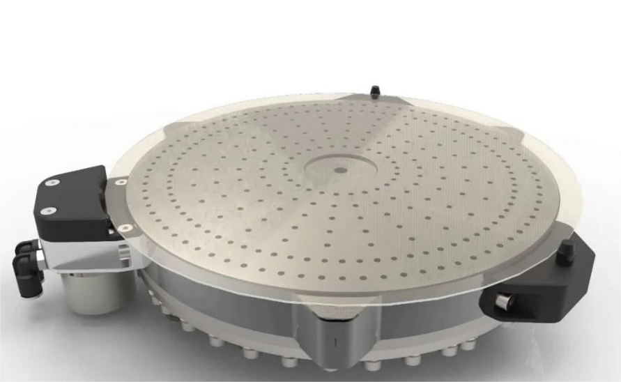
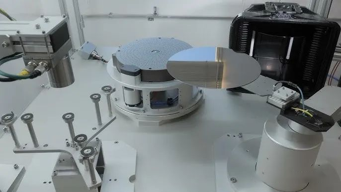
The pin (adsorption pin) function of the vacuum adsorption disk
pin provides a uniform support point to ensure that the wafer remains flat during the adsorption process, avoiding bending or cracking due to uneven forces.
The precise pin design ensures that the wafer is accurately aligned and placed in the intended position on the chuck, providing precise positioning for subsequent machining processes.
Advantage
Reliability: Mechanical vacuum adsorption provides a stable adsorption force to ensure wafer stability during processing.
Versatility: This method is suitable for different sizes and types of wafers, and has high flexibility.
Maintenance is relatively simple: mechanical vacuum adsorption systems are easier to maintain.
Defect
Potential damage risk: If the vacuum fails or is operated improperly, the wafer may be damaged.
Sensitivity: For extremely fragile or ultra-thin wafers, mechanical vacuum adsorption may not be the best choice.
Electrostatic adsorption
Electrostatic adsorption (ESC) usually consists of an absorber surface, an electrode and a power supply made of an insulating material. The electrode is embedded below the adsorption surface, and the insulating material is used to isolate the electrode from the adsorbed object. By applying a voltage to the electrode, an electric field is generated. This electric field passes through the adsorption surface and is induced on the wafer, creating an electrostatic attraction between the wafer and the adsorption surface. The free charge on the wafer is attracted to one side of the electric field, which creates an attraction to the adsorption surface.
Advantages:
Electrostatic adsorption does not require physical contact with the wafer, thus reducing the risk of mechanical damage and contamination.
By changing the applied voltage, the size of the adsorption force can be precisely controlled to adapt it to different applications and process requirements.
Once the wafer is absorbed, even if the power is off, the adsorption force will be maintained for a period of time, and there is no need to worry about the wafer falling down.
Bernoulli Chuck
The Bernoulli Chuck is a wafer adsorption device based on the Bernoulli principle. Bernoulli's principle states that when a fluid flows along a flow line, the pressure decreases as the fluid speed increases, and vice versa.
In Bernoulli Chuck, gas flows out of the nozzle at high speed and along the surface of the wafer. Due to this high-speed airflow, the pressure on the wafer surface is reduced, creating a pressure difference between the wafer and Chuck. This pressure difference causes the wafer to be attracted to the Chuck, but it is also suspended above the airflow, thus reducing physical contact with the Chuck.
Advantages:
Bernoulli chuck make little physical contact between the wafer and the suckers. This helps reduce potential mechanical damage and contamination.
Using inert gas as an air cushion, it can work stably in various temperature and chemical environments.
The airflow can be adjusted to accommodate wafers of different sizes and shapes.
Defect:
Higher cost
High requirements on wafer flatness
A little louder
Fountyl Technologies PTE Ltd, is focusing on semiconductor manufacturing industry, main products include: Pin chuck, porous ceramic chuck, ceramic end effector, ceramic square beam, ceramic spindle, welcome to contact and negotiation!