


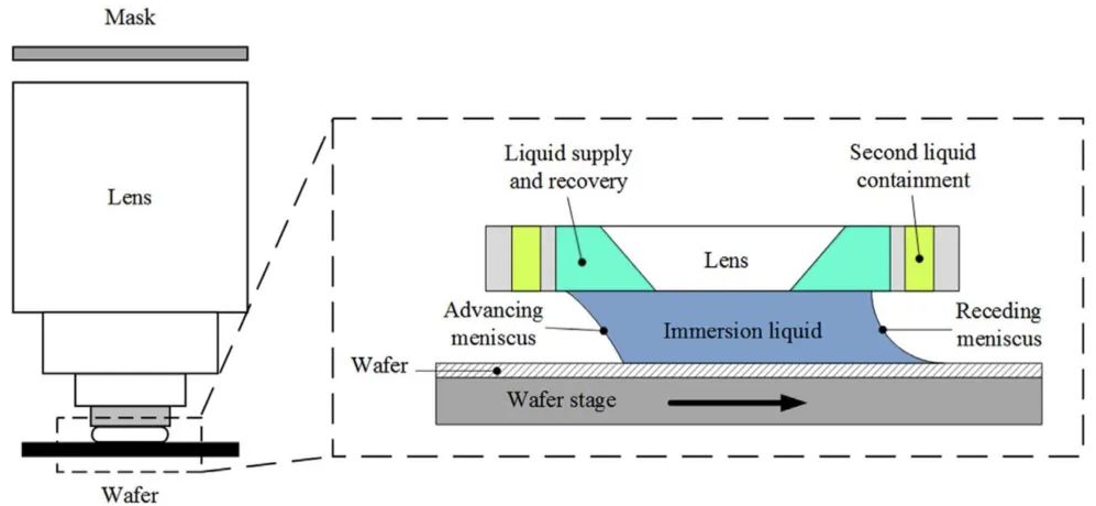
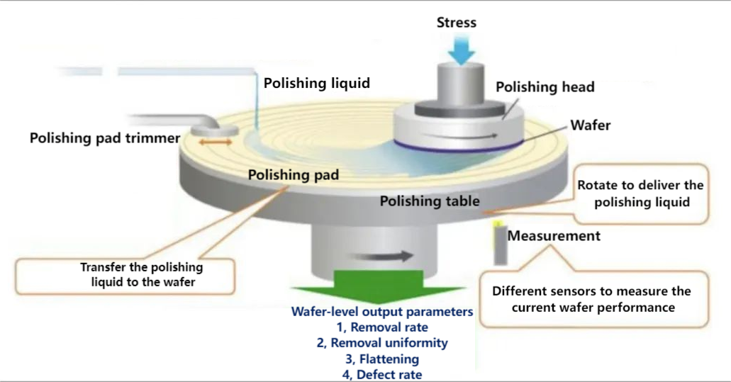
News
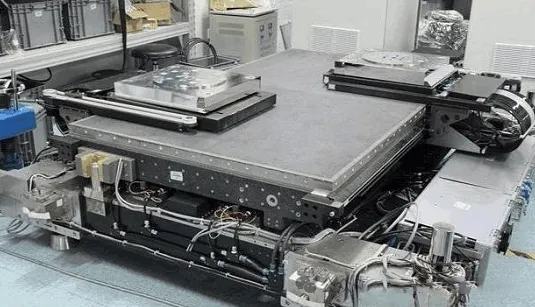
Common wafer slicing methods
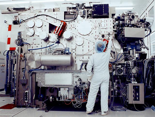
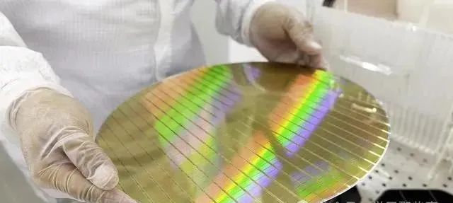
Wafer scribing, as a key step in semiconductor manufacturing, directly affects the quality and output of the chip. The process involves cutting a single silicon wafer into thousands of tiny pieces, each of which is a chip. With the continuous progress of science and technology, wafer scribing methods are also constantly developing and innovating, the following are several mainstream wafer scribing methods.
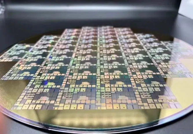
Wafer scribing: Evolution of cutting technology Wafer scribing is the process of cutting a single wafer into thousands of individual chips. This step takes place after the wafer has completed all semiconductor manufacturing processes so that each chip can be individually packaged and used.
Traditionally, we have two mainstream scribing methods: mechanical scribing and laser scribing.
Mechanical scribing: This is a method of physically cutting a wafer using a diamond blade, and is the most traditional and widely used scribing technology. Its advantage is that the equipment cost is relatively low, and it is suitable for wafers of a variety of materials. However, the accuracy of mechanical scribing is not high, and it is prone to problems such as low scribing rate and edge breakage, especially for wafers with a thickness of more than 100um.
Laser scribing: With the advancement of technology, laser scribing has gradually become a more advanced option. It mainly includes two ways: laser hidden cutting and laser full cutting. Laser hidden cutting technology can achieve high precision slicing by forming a fine crack inside the wafer, while keeping the surface intact. Laser full cutting is directly through the entire wafer thickness to achieve one-step cutting. The advantages of laser scribing are fast scribing speed, small stress damage and high accuracy, but the cost is relatively high.
Innovative processes: DBG and slotted Scribing In addition to the above traditional scribing methods, there are also some innovative processes on the market. such as DBG (Dicing Before Grinding) and grooving cutting technology. The DBG process is to first slice the front of the wafer to a specified depth, and then grind the back of the wafer to the corresponding depth, thereby reducing the problem of wafer breakage. Slotting is first slotted with a laser or thick diamond blade, and then carefully slotted to reduce the problem of edge breakage and improve the quality of scribing. With the continuous development of semiconductor technology, the wafer slicing process is also improving. The future slicing technology will pay more attention to the balance of accuracy, efficiency and cost to meet the growing market demand. Whether through the improvement of existing technology, or the development of new slicing methods, wafer slicing technology innovation will bring a broader development space for the semiconductor industry.
As explorers at the forefront of science and technology, let us look forward to the future development and breakthrough of wafer slicing technology, and believe that in the near future, this core technology will lead the semiconductor industry to a higher peak. Join my knowledge community, let's witness the power of technology and explore more unknown wonders.
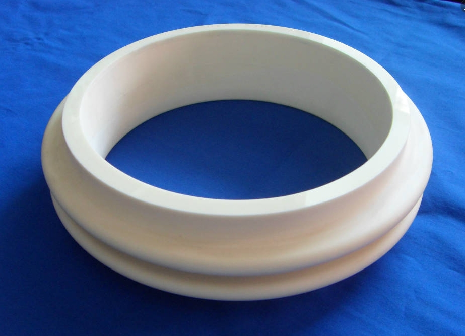
Fountyl Technologies PTE Ltd, is focusing on semiconductor manufacturing industry, main products include: Pin chuck, porous ceramic chuck, ceramic end effector, ceramic square beam, ceramic spindle, welcome to contact and negotiation!