


News

How to solve the chip package heat dissipation problem
Advanced packaging chips can not only meet the needs of high-performance computing, artificial intelligence, power density growth, etc., but also the heat dissipation problem of advanced packaging has become complicated. Because hot spots on one chip affect the heat distribution of neighboring chips. The interconnections between chips are also slower in modules than in SoCs.
John Parry, industry head of electronics and semiconductors at Siemens Digital Industry Software, said: "Before the world moved into areas like multi-core, you were dealing with a chip that had a maximum power of about 150 watts per square centimeter, which was a single point heat source. You can dissipate heat in all three directions, so you can achieve some pretty high power densities. But when you have a chip, put another chip next to it, and then put another chip next to it, they heat each other up. That means you can't tolerate each chip having the same power level, which makes the thermal challenge much more difficult."
This is one of the main reasons why 3D-IC stacking is making slow progress in the market. While the concept makes sense from a power efficiency and integration standpoint - and works well in 3D NAND and HBM - it's a different story when logic is included. The logic chip generates heat, and the denser the logic, the higher the utilization of the processing elements, the greater the heat. This makes logical stacking rare.
Choose the right package
For chip designers, there are many ways to package. But the performance of chip integration is crucial. Components such as silicon, TSV, and copper columns all have different coefficient of thermal expansion (TCE), which affects assembly yield and long-term reliability.
The current popular flip BGA package with cpu and HBM has an area of about 2500 square millimeters. Mike McIntyre, head of software product management at Onto Innovation, said: "We're seeing a big chip potentially becoming four or five small chips. So you have to have more I/O in order for these chips to talk to each other. So you can distribute the heat. Ultimately, heat dissipation is a problem that can only be dealt with at the system level, and it comes with a series of trade-offs.
In fact, some devices are so complex that it is difficult to easily replace components in order to customize these devices for applications in specific fields. This is why many advanced packaging products are for very high-volume or price-elastic components, such as server chips.
Progress in chip module simulation and testing
Nevertheless, engineers are looking for new ways to perform thermal analysis of package reliability before the packaged modules are manufactured. For example, Siemens provides an example of a dual ASIC based module that installs a fan-out redistribution layer (RDL) on a multilayer organic substrate in a BGA package. It uses two models, one for RDL-based WLP and the other for multi-layer organic substrate BGA. These packaging models are parameterized, include substrate stacking and BGA before EDA information is introduced, and enable early material evaluation and chip placement selection. Next, the EDA data is imported, and for each model, the material map is able to provide a detailed thermal description of the copper distribution in all layers.
Eric Ouyang, Director of Technical Marketing at JCET, together with engineers from JCET and Meta, compared the thermal performance of single-chip, multi-chip modules, 2.5D plugboards and 3D stacked chips with one ASIC and two Srams. [1] The Apple-to-Apple comparison leaves the server environment, radiator with vacuum chamber, and TIM unchanged. In terms of heat, 2.5D and MCM perform better than 3D or single-chip chips.
Quantized thermal resistance
We can understand how heat is conducted through silicon chips, circuit boards, glues, TIMs or packaging caps, while using the standard method of temperature difference and power function to track temperature and resistance values.
"The thermal path is quantified by three key values - the thermal resistance from the device node to the environment, the thermal resistance from the node to the housing [at the top of the package], and the thermal resistance from the node to the board," says JCET's Ouyang. At the very least, he points out, JCET's customers need ɵja, ɵjc and ɵjb, which they then use in system design. They may require that a given thermal resistance does not exceed a specific value and that the package design provide that performance.
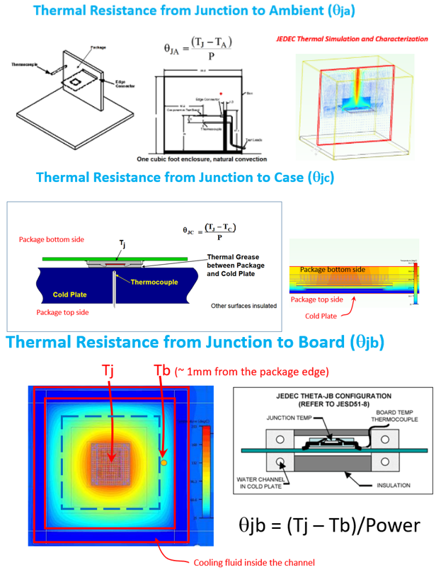
Thermal simulation is the most economical way to explore the selection and collocation of materials. Through the simulation of the chip in the working state, we usually find one or more hot spots, so we can add copper to the substrate below the hot spot to facilitate heat dissipation; Or change the packaging material, increase the radiator. The system integrator may specify that the thermal resistance ɵja, ɵjc, and ɵjb must not exceed certain values. Under normal circumstances, the silicon junction temperature should be kept below 125 ° C. After the simulation is complete, the packaging plant conducts a design of experiments (DOE) to arrive at the final package plan.
Select TIM
In the package, more than 90% of the heat is dissipated through the package from the top of the chip to the radiator, which is usually a vertical fin based on anodized aluminum. Thermal interface materials (TIM) with high thermal conductivity are placed between the chip and the package to help transfer heat. Next-generation TIM for cpus include sheet metal alloys such as indium and tin, as well as silver-sintered tin with conductivity of 60W/m-K and 50W/m-K, respectively. As vendors transition SoCs to chiplet processes, more TIMs with different properties and thicknesses are needed.
YoungDo Kweon, senior director of research and development at Amkor, said that for high-density systems, the thermal resistance of the TIM between the chip and the package has a greater impact on the overall thermal resistance of the packaged module. Power trends are increasing dramatically, especially for logic, so we focus on keeping the junction temperature low to ensure reliable semiconductor operation. While TIM suppliers provide thermal resistance values for their materials, in reality, the thermal resistance from chip to package (ɵjc) is affected by the assembly process itself, including the bonding quality and contact area between the chip and TIM. He notes that testing with actual assembly tools and bonding materials in a controlled environment is critical to understanding actual thermal properties and selecting the best TIM for customer verification.
To deal with heat in different ways
Chip makers are looking for ways to solve the heat dissipation problem. Randy White, program manager for memory solutions at Keysight Technologies, said: "The package is the same, if you reduce the chip size area by a quarter, it will speed up. This may result in some signal integrity differences. Because the bonding line of the external package will enter the chip, the longer the line, the greater the inductance, so there is an electrical performance part. So how do you consume that much energy in a small enough space? This is another key parameter that needs to be studied." This has led to significant investment in cutting-edge bonding research that seems to focus on hybrid bonding. But the cost of hybrid bonding is high, and it is still limited to high-performance processer-type applications, with TSMC being one of the only companies currently offering this technology. However, the prospect of combining photons on CMOS chips or silicon-based gallium nitride is very promising.
Fountyl Technologies PTE Ltd, is focusing on semiconductor manufacturing industry, main products include: Pin chuck, porous ceramic chuck, ceramic end effector, ceramic square beam, ceramic spindle, welcome to contact and negotiation!