


News
Improved gallium nitride substrate thinning technology
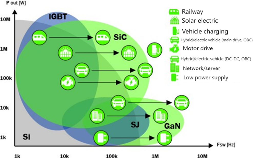
Switching to a hydrogen-based plasma ensures high-speed etching of GaN substrates, and engineers at Osaka University in Japan claim to have made a new breakthrough in thinning gallium nitride (GaN) substrates using hydrogen-based plasma. The team's technique, with etching rates up to 4μm/ min, provides a viable way to thin substrates for vertical power devices. This is necessary to reduce the on-resistance of vertical devices so that they can win the competition in electric vehicles.
The Osaka University team pioneered a compelling alternative to existing machining processes, such as grinding and polishing, both of which are used today to thin substrates. These mechanical methods work well in thinning silicon power devices, but are less effective in thinning materials such as silicon carbide and gallium nitride due to problems such as cracking, edging and warping.
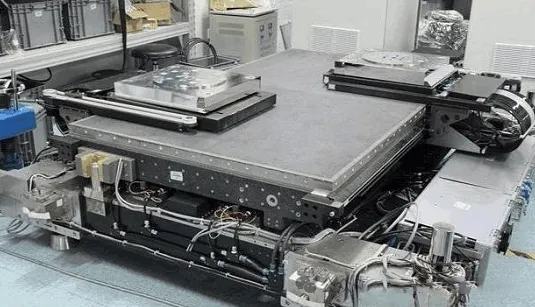
To thin the GaN substrate, engineers at Osaka University employed a method called plasma chemical gasification processing (PCVM), which they have been using and improving for more than 25 years. "Initially, we were dealing with silicon wafers for synchrotron radiation, SOI wafers and silicon X-ray mirrors," said Yasuhisa Sano, a team spokesperson. They started processing SiC substrates about 15 years ago and GaN and Ga2O3 substrates in recent years. A notable feature of PCVM is the use of plasma pressures of several tenths of an atmosphere, which ensures a short average path of gas molecules and low energy of ions. Therefore, the reactant is not an ion, but a neutral free radical, which does not destroy the atomic arrangement of the machined surface, nor does it deform the substrate.
Back in 2021, Sano and colleagues reported using SF6 gas to thin a 2-inch SiC substrate through PCVM at a rate of 15μm/ min. Unfortunately, this method cannot be directly applied to GaN, because SF6 gas does not ensure the etching effect. Chlorine-based gases are also unsuitable as obvious contenders because they are corrosive and have the potential to damage the surface of gallium nitride devices. These questions prompted the team to consider using hydrogen. The use of hydrogen in the HVPE growth of gallium nitride, as well as the presence of Ga2H6 gas, are all positive factors for possible success.
Studies involving hydrogen began with a homemade 13.56 MHz RF plasma generator consisting of a tubular electrode with an outer diameter of 2 mm and a aperture of 0.3 mm and a 2-inch GaN substrate with a thickness of 0.4 mm. Initially, the team used a 9:1 helium-hydrogen ratio, a flow rate of 100 sccm, and RF power of 130 W, 150 W, 180 W, and 200 W to study the changes in removal rates after five minutes. The experiment also took into account the substrate temperature and determined that the higher power was the main driver of the improved removal rate - it increased the number of hydrogen free radicals.
Sano and colleagues continued to account for the effects of gas flow rates, with the power fixed at 180 W. They compared etching rates at 100 sccm, 500 sccm, and 800 sccm flows, this time with a helium-hydrogen ratio of 19:1, which, according to preliminary studies, speeds up the etching process. At the highest flow rate, the etching speed reaches 4μm/ min, but the surface quality is affected, forming the so-called pear skin surface (see figure).
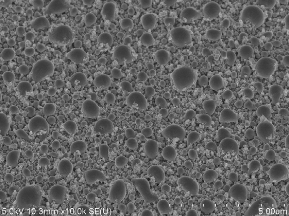
Scanning electron microscopy showed gallium deposits on the surface at a flow rate of 100 sccm. The team attributes this morphology to spherical deposits of gallium, which can be removed simply by heating the surface to 40°C and then wiping it down. But there is a more elegant solution: adding oxygen to the process. Atomic force microscopy showed that the introduction of oxygen ensured a smooth surface with a roughness of only 0.9 nm.
Sano said the research team is now trying to establish the process conditions to obtain good surface roughness. "At the same time, we are working on processing larger areas to bring our technology closer to practical applications."
FOUNTYL TECHNOLOGIES PTE. LTD. is a modern enterprise in the field of advanced ceramics set R&D, manufacturing and sales as one, mainly produces porous ceramics, alumina, zirconia, silicon nitride, silicon carbide, aluminum nitride, microwave dielectric ceramics and other advanced ceramic materials. our specially invited Japanese technology expert have more than 30 years of industry experience in semiconductor field, efficiently provide special ceramic application solutions with wear resistance, corrosion resistance, high temperature resistance, high thermal conductivity, insulation for domestic and foreign customers.