


News

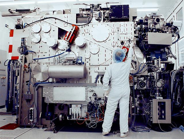
Progress has been made in the study of 8-inch silicon carbide single crystals
The characteristics of high-quality crystal quality of SiC epitaxial layer make the epitaxial layer should have a crystal structure of high purity and low defect density to ensure the reliability of SiC components. The surface of the epitaxial layer with good surface topography should be flat and smooth, without obvious steps and impurity particles, which helps to improve the stability of SiC components. The doping elements in the epitaxial layer should be evenly distributed, which can ensure the electrical performance of the SiC components is consistent. In order to obtain high quality SiC epitaxial layer, advanced growth technology and process control are required. At the same time, the epitaxial layer is also needed.
Silicon carbide (SiC) is a wide band gap compound semiconductor with high breakdown field strength (about 10 times that of Si), high saturated electron drift rate (about 2 times that of Si), and high thermal conductivity (3 times that of Si and 10 times that of GaAs). Compared with similar silicon-based devices, SiC devices have the advantages of high temperature resistance, high voltage resistance, high frequency characteristics, high conversion efficiency, small size and light weight, etc., and have important application potential in electric vehicles, rail transit, high voltage power transmission and transformation, photovoltaic, 5G communication and other fields. High quality, low cost and large size SiC single crystal substrate is the basis for preparing SiC devices, and mastering the SiC crystal growth and processing technology with independent intellectual property rights has been the focus of research in related fields.
Since 1999, the research team of Chen Xiaolong, Key Laboratory of Advanced Materials and Structural Analysis, Institute of Physics, Chinese Academy of Sciences/Beijing National Research Center for Condensed Matter Physics, based on independent innovation, has systematically studied the basic laws of thermodynamics and growth dynamics of SiC crystal growth with self-developed growth equipment, and understood the formation mechanism of phase transition and defects during crystal growth. Proposed defect, resistivity control and expansion methods, formed a series of key technologies from growth equipment to high-quality SiC crystal growth and processing, and continuously increased the diameter of SiC crystals from less than 10 mm (2000) to 2 inches (2005). In 2006, the team took the lead in the industrialization of SiC single crystals in China, successfully transformed the research results in Beijing Tianke Heda Semiconductor Co., LTD., and successfully developed 4-inch (2010) and 6-inch (2014)SiC single crystals through the combination of industry, university and research. At present, Beijing Tianke Heda has realized the mass production and sales of 4-6 inch SiC substrates, and has become one of the main suppliers of international SiC conductive wafers.
The cost of SiC device is mainly formed by the substrate, epitaxial, flow plate and sealing and other links, and the substrate accounts for as high as 45% of the cost of SiC device. In order to reduce the cost of a single device and further expand the SiC substrate size, increasing the number of devices on a single substrate is the main way to reduce the cost. An 8-inch SiC substrate will have a significant cost reduction advantage over a 6-inch one. It has been reported that the international 8-inch SiC single crystal substrate has been successfully developed, but no products have been put on the market so far.
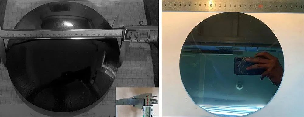
The difficulty of 8-inch SiC crystal growth lies in: first of all, 8-inch seed crystal must be developed; Secondly, it is necessary to solve the problem of uneven temperature field and gas phase material distribution and transport efficiency caused by large size. In addition, it is necessary to solve the problem of crystal cracking caused by increased stress. On the basis of existing research, in 2017, researcher Chen Xiaolong, doctoral student Yang Naiji, associate researcher Li Hui, and Chief engineer Wang Wenjun began to study the 8-inch SiC crystal. Through continuous research, they mastered the room temperature field distribution and high temperature gas phase transport characteristics of 8-inch growth. Using 6-inch SiC as seed crystal, they designed a device conducive to the expansion and growth of SiC. The problem of polycrystalline nucleation at the edge of seed crystals in the process of expanding diameter is solved. A new type of growth device is designed to improve the efficiency of raw material transportation. Through many iterations, the size of SiC crystal is gradually expanded. By improving the annealing process, the stress in the crystal is reduced and the cracking of the crystal is inhibited. An 8-inch SiC crystal was initially grown on a self-developed substrate in October 2021.
The successful development of 8-inch SiC conductive single crystal is another landmark progress made by the Physics Institute in the field of wide band gap semiconductors. After the transformation of the research and development results, it will help enhance the international competitiveness of China's SiC single crystal substrate and promote the rapid development of China's wide band gap semiconductor industry.
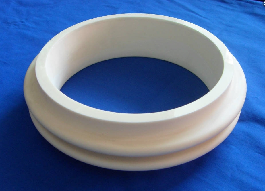
FOUNTYL TECHNOLOGIES PTE. LTD. is a modern enterprise in the field of advanced ceramics set R&D, manufacturing and sales as one, mainly produces porous ceramics, alumina, zirconia, silicon nitride, silicon carbide, aluminum nitride, microwave dielectric ceramics and other advanced ceramic materials. our specially invited Japanese technology expert have more than 30 years of industry experience in semiconductor field, efficiently provide special ceramic application solutions with wear resistance, corrosion resistance, high temperature resistance, high thermal conductivity, insulation for domestic and foreign customers.