


News

The type and package of the chip
Integrated circuit (IC) is the cornerstone of modern electronic technology. They are the heart and brain of most circuits. They are everywhere and you can find them on almost every circuit board.
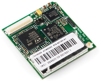
An integrated circuit is a collection of electronic components: resistors, transistors, capacitors, etc., all crammed into a small chip and connected together to achieve a complex functional goal. They have many functional categories: circuit logic gates, operational amplifiers, timers, regulators, circuit controllers, logic controllers, microprocessors, memory... etc.
Internal IC
The inside of a chip is a complex circuit structure composed of silicon wafers, copper and other materials, which are connected to each other to form resistors, capacitors, transistors or other components in the circuit. Chips are initially made on round silicon wafers, and after the wiring is completed, the wafers are cut into small pieces to form the chip. The chip itself is small, and the semiconductor chip and copper layer it consists of are very thin. The connections between the layers are complex.
A chip is the smallest unit of an application circuit. Because the chips are too small to be welded or joined. In order to make the work of connecting the circuit to the chip easier, the chip packaging technology needs to be used. Chip packaging technology turns small, delicate silicon chips into the black chips we are all familiar with.
IC packaging
Packaging technology makes a finished chip and extends it to make it easier to connect structures with other circuits. Each external connection on the chip is connected via a small length of gold wire to a pad or pin on the package. The pin is the silver squeeze terminal on the chip circuit, which continues to connect to the rest of the circuit. There are many different types of packages, each with a unique size, mounting type, and/or number of pins. The figure below lists dozens of chip packages, each with its own unique name. Some of the major packaging categories are discussed in detail in the following articles.
Polarity marker and pin number
All chips are marked with polarity, and the position and function of each pin is unique. This means that the package must have some way of defining the functionality of each pin. Most chips will use a notch or a Dot to indicate which pin is first. (sometimes both), once you know where the first pin is, the rest of the pin code is incremented counterclockwise on the chip.
Installation mode
One of the main distinguishing features of chip package types is the way they are mounted onto the circuit board. All packages fall into one of these two mounting types: through hole (PTH) or surface mount (SMD or SMT). Through-hole packages are generally larger and easier to use. They are designed to pass through one side of the board and then solder to the other side. The surface patch package is designed to be located on the same side of the board and is welded to the board surface. The pins of the SMD package should be of two kinds, one is drawn from the side, perpendicular to the chip; The other is located at the bottom of the chip and arranged in a matrix. This form of component is not quite "suitable for manual assembly". They often require special tools to assist in this process.
We do a detailed illustration of various common chip packaging forms of below:
Dual in-line package (DIP)
DIP, short for dual in-line package, is the most common through-hole IC package. These tiny chips have two rows of parallel pins and a rectangular black plastic shell protrudes vertically.
SMD/SMT:Surface-Mount
There are now a wide variety of surface mount package types. It is usually necessary to make a wiring pattern matching the chip on the PCB in advance and weld it. The installation of SMT is usually a device that requires automation.
SOP:Small Outline Package
SOP packaging is an evolved form of surface mount for DIP. If all the pins on the DIP are bent outward and then reduced to the appropriate size, a single-sided mounted SOP can be formed. This package is one of the easiest SMD parts to solder by hand. On SOIC (Small-outline IC) packages, each pin is typically separated by about 0.05 inches (1.27 mm). SSOP(shrink small-outline package) is a scaled-down version of SOIC packaging. Other similar IC packages include TSOP(thin small-outline package) and TSSOP(thin shrink smalloutline package).
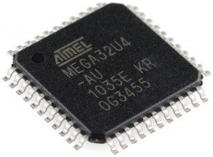
QFP (Quad Flat Package)
Unfold the IC pins in all four directions to look like a four-sided flat package (QFP). QFP ics may have 8 pins per side (32 in total) to 70 pins per side (more than 300 in total). The pin spacing on a QFP IC is usually between 0.4mm and 1mm. There are some miniaturized variations of the standard QFP, thin QFP(TQFP: thin QFP), Very Thin Thin (VQFP), and Low Configuration (LQFP) packages.
QFN (Quad Flat No-leads)
Removing the pins of the QFP IC and shrinking the pins onto the corners of the four sides gives you something that looks like a Quad-Flat No-leads (QFN) package. The connector on the QFN package is much smaller, exposed at the bottom edge of the IC.
Thin (TQFN), Ultra-thin (VQFN), and Micro-lead (MLF) packages are variants of the standard QFN package. There are even dual no-lead (DFN) and thin dual no-lead (TDFN) packages with pins on only two sides. Many microprocessors, sensors, and other new ics come in QFP or QFN packages. The popular ATmega328 microcontroller is available in TQFP package and QFN type (MLF) form, while micro accelerometers/gyroscopes like the MPU-6050 are available in micro QFN form.
Ball Grid Arrays
Finally, for truly advanced integrated circuits, there are ball-grid array (BGA) packages. This is a complex and subtle package in which small solder balls are arranged in a two-dimensional grid at the bottom of the IC. Sometimes the solder ball is attached directly to the chip!
BGA packages are typically used on advanced microprocessors. If you can manually weld a bga encapsulated IC, you can consider yourself a master welder. Typically, placing these packages on the PCB requires an automated process that includes a take-and-place machine and a reflux furnace.
Common IC
Integrated circuits are ubiquitous in electronics in so many forms that it is difficult to cover everything. Here are some of the more common ics you may encounter in electronics.
1, Logic gate, timer, shift register.
As building blocks of more integrated circuits themselves, logic gates can be packaged into their own integrated circuits. Some logic gate ics may contain a small number of gates in a package, and logic gates can be connected within integrated circuits to create timers, counters, latches, shift registers, and other basic logic circuits. Most of these simple circuits can be found in DIP packages, as well as SOIC and SSOP.
2, Microcontrollers, microprocessors, FPGAs
Microcontrollers, microprocessors, and FPGAs are all integrated circuits that pack thousands, millions, or even billions of transistors into a small chip. These components are functionally complex and vary widely in size. From 8-bit microcontrollers, such as the ATmega328 in Arduino, to complex 64-bit multi-core microprocessors, these are components that are widely used in computers. These components are also usually the largest integrated circuits in the circuit. Simple microcontrollers can be found in packages from DIP to QFN/QFP, with pin counts ranging from 8 to 100. As the complexity of these components increases, so does the complexity of packaging. FPGAs and complex microprocessors can have more than a thousand pins and can only be used in advanced packages such as QFN, LGA or BGA.
3, Sensor
Modern digital sensors such as temperature sensors, accelerometers, and gyroscopes are all integrated in one integrated circuit. These ics are typically smaller than other ics on microcontrollers or boards, with pin counts in the range of 3 to 20. Now in the large control chip, many sensors will be directly integrated in it.
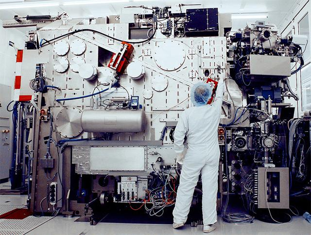
Fountyl Technologies PTE Ltd, is focusing on semiconductor manufacturing industry, main products include: Pin chuck, porous ceramic chuck, ceramic end effector, ceramic square beam, ceramic spindle, welcome to contact and negotiation!