


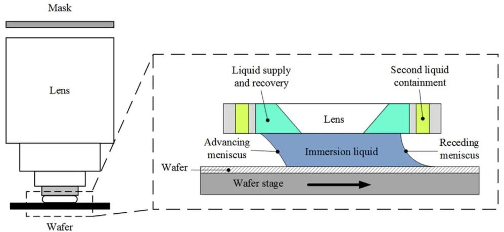
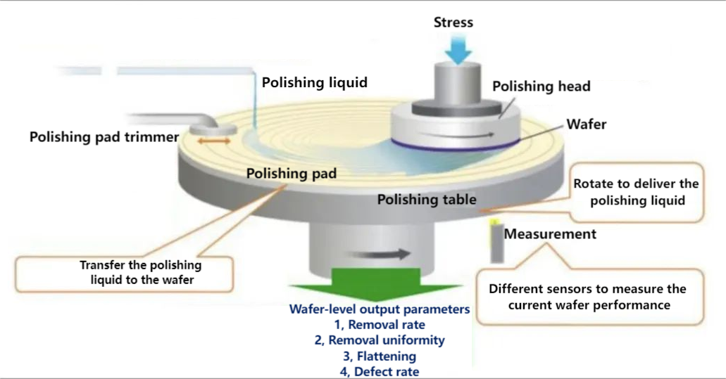
News

Why are chips square and wafers round?
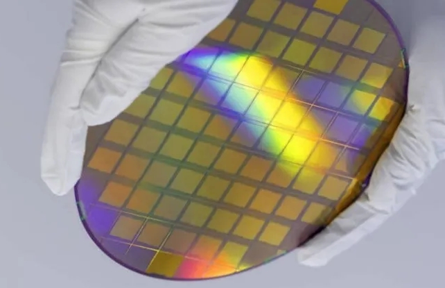
In the public impression, the wafer is a thin, round high-purity silicon wafer, and on this high-purity silicon wafer can be processed to produce a variety of circuit component structures, so that it becomes an integrated circuit product with specific electrical functions. The densely packed components are neatly placed on a monocrystalline silicon material, which is orderly and square. It can be seen that wafers are still cut into squares in practical applications.
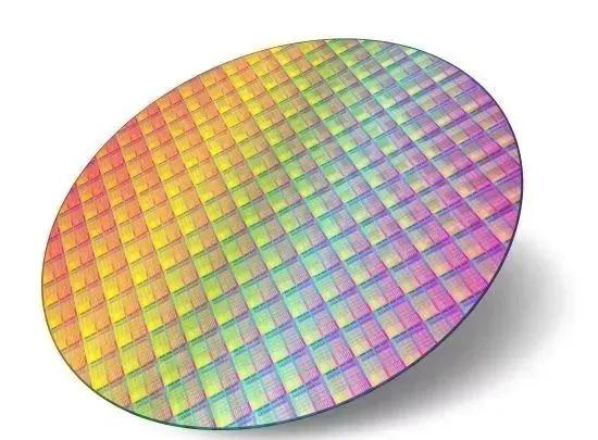
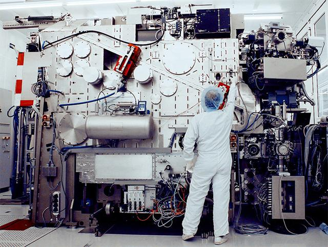
Why are silicon wafers made round? Why is it "wafer" and not "crystal square"? Why is there no chip in the outer ring of some wafers, and some wafer circuits are laid on the whole wafer, and there will be incomplete chips in the outer ring of the wafer? Friends who are familiar with the semiconductor manufacturing process know that before the chip is cut and packaged, all the manufacturing process is operated on the Wafer. But the chips we see are all square, and when you make a chip on a round wafer, there will always be some areas that are not utilized. So why not use square wafers to increase utilization? Because wafers (originally silicon wafers) are cut from cylindrical silicon rods, the cross section can only be circular.
Wafers are better suited to making chips than "crystal squares"
Silicon wafer manufacturing can be summarized into three basic steps: silicon refining and purification, monocrystalline silicon growth, wafer molding.
The first is the purification and melting of silica sand. At this stage, polysilicon is mainly obtained through a series of measures such as dissolution, purification and distillation.
Next is the monocrystalline silicon growth process. It is the growth of monocrystalline silicon from silicon melt. High purity polysilicon is placed in a quartz crucible and heated at high temperatures in a protective atmosphere to melt it. Large diameter monocrystalline silicon ingot can be drawn vertically by using a small seed crystal slowly rising from the rotating melt.
The final step is wafer molding. Monocrystalline silicon ingot is generally cylindrical, ranging from 3 inches to more than 10 inches in diameter. After the silicon ingots are sliced and polished, a monocrystalline silicon wafer, also known as a wafer, is obtained.
At present, the Czochralase method is the most commonly used method to grow wafers, in addition to the Czochralase method, the commonly used method is also zone melting. All in all, the monocrystalline silicon rod is cylindrical, and the monocrystalline silicon wafer obtained by this method is naturally round. In fact, the silicon rod can be cut into a cuboid before being sliced, so that the "crystal square" can be directly obtained when being sliced later. But the silicon rods used to make chips don't do this, for several reasons:
The first is that the round is more suitable for photoresist coating. in addition, due to the existence of edge stress, the structural strength of circular wafers is also higher than that of square wafers. The silicon wafer needs to undergo multiple photoliths, etchings, chemical grinding and other processes before becoming a wafer, and the wafer will accumulate more stress in the outer ring. Therefore, the sharp Angle of the square will cause the edge stress concentration, which is easily damaged in the production process and affects the overall yield.
In general, round wafers are more convenient for chip manufacturing and have higher yields. If the wafers used to make chips are not convenient to make square, why can't chips be made round?
Round chips are harder to make
After the silicon wafer is coated, lithography, etching, ion injection and other steps, a chip will be manufactured, but at this time the chip is still "long" on the wafer, and needs to be cut to become a separate chip.
The square chip can be cut off with just a few cuts. Round chips, I am afraid it will take several times more time than square to cut. Most importantly, round chips do not solve the problem of wasted silicon area.
In fact, saving wafer area is always an important issue. The more chips that can be produced on a wafer, the higher the production efficiency and the lower the cost of a single chip. At present, the best way to solve the production efficiency is to increase the wafer area, which is the familiar calculus.
Square photovoltaic silicon wafer
In addition to making chips, silicon wafers are also an extremely important part of the photovoltaic field.
Solar panel structure (the cell is silicon)
The early stage of the preparation process of photovoltaic monocrystalline silicon is the same as chip monocrystalline silicon, the reason for the square is also very simple, if the photovoltaic cell is round, multiple cells arranged into the middle of the solar panel will appear gaps, reducing the overall conversion rate. Compared with the chip, the silicon purity requirements for the manufacturing of photovoltaic panels are slightly lower, and the purity standard only needs to be 99.9999%, which can not reach the 99.9999999% of the production of chips.
***SUMMARIZE***
Why are chips square? Round chips are difficult to cut, the subsequent packaging stage is not convenient to control, and most importantly, round chips can not solve the problem of wasted wafer area. Why are wafers round? In the process of producing chips, circular wafers are more convenient to produce due to mechanical factors, and the yield is higher, and the silicon rod is naturally cylindrical, and the wafer is naturally round. However, in the photovoltaic field, the square silicon wafer does not waste space when the battery is packaged, so the photovoltaic silicon wafer is square.
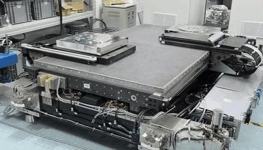
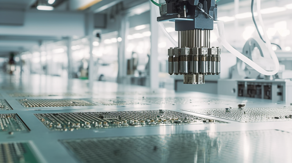
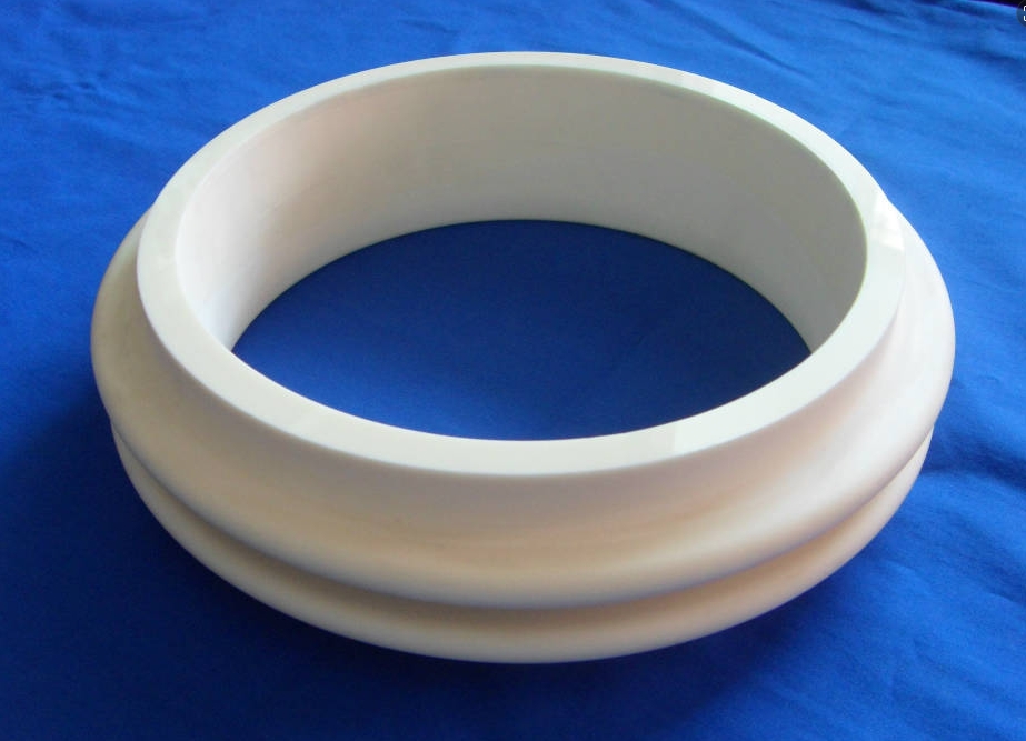
Fountyl Technologies PTE Ltd, is focusing on semiconductor manufacturing industry, main products include: Pin chuck, porous ceramic chuck, ceramic end effector, ceramic square beam, ceramic spindle, welcome to contact and negotiation!