

Wafer pin silicon carbide chuck
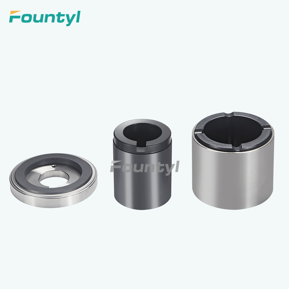
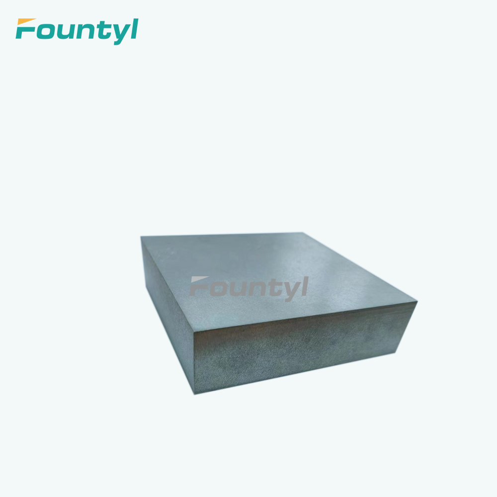
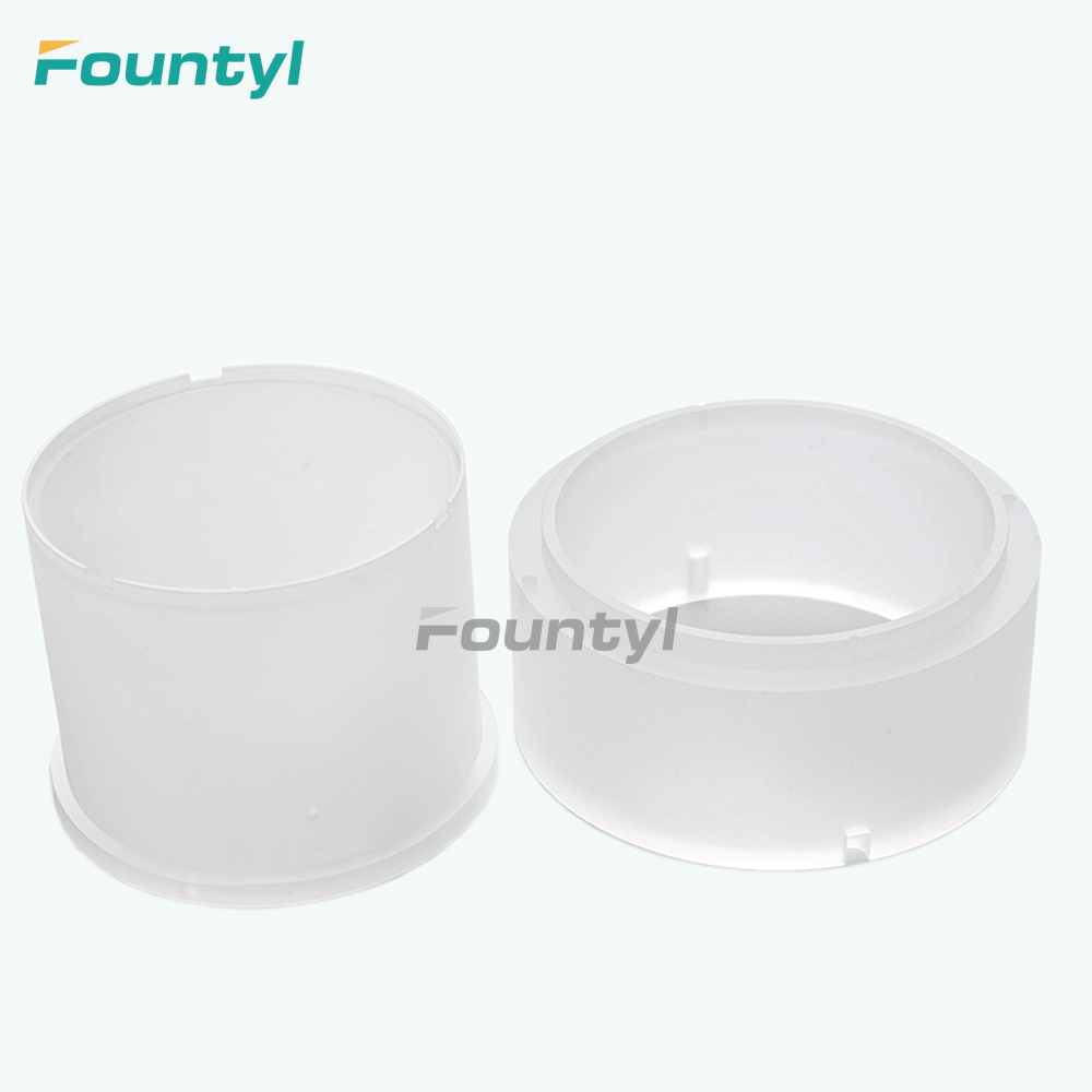
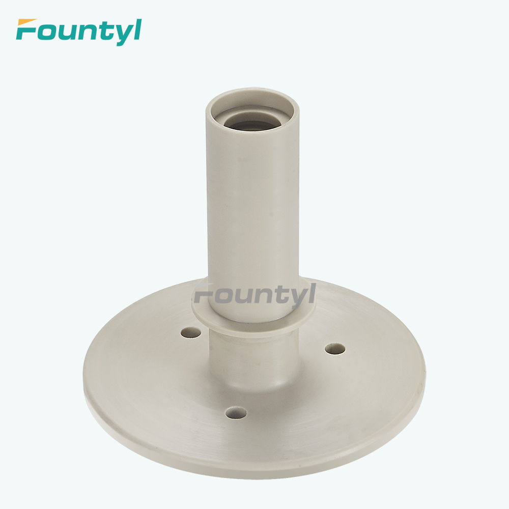
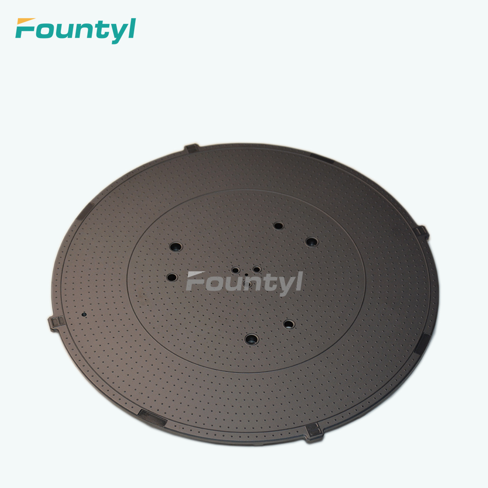
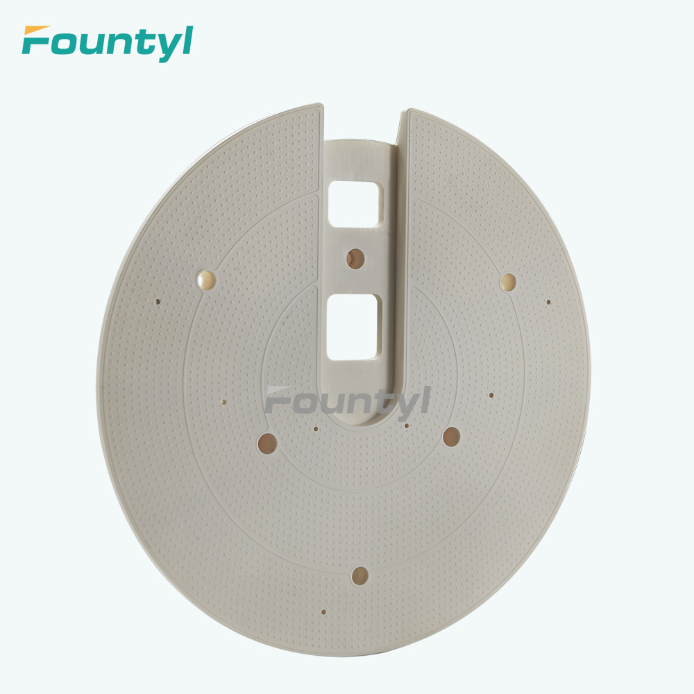
Wafer pin silicon carbide chuck(wafer clamping, prealigner chuck) used for semiconductor field
Features
High temperature resistance: Silicon carbide and alumina ceramic
materials have excellent high temperature performance, can be used in high temperature environment for a long
time, not easy to deformation or fracture.
Corrosion resistance: can withstand a variety of chemical corrosion,
suitable for handling corrosive liquids or gases in the working environment.
Wear resistance: high hardness, with good wear resistance, can be used
for a long time without failure.
Strong adsorption: the convex point structure reduces the contact area
of the suction cup, thereby increasing the adsorption force per unit area, and can more firmly adsorb the
workpiece.
High stability: Due to the characteristics of the material, the wafer
pin chuck has high stability and can work stably for a long time.
Reduce pollution: Ceramic wafer chucks are evolving from grooves to
pins to reduce contact area, reduce some pollution and improve warping correction.
Process Control
High precision: 12 inches diameter, flatness is controlled within 5 μm; If you need more precision, please
email us.
Shape control: Adjust the chuck shape according to the wafer shape (non-uniformity control).
Absorptive responsiveness: Customized design according to specifications.
Our Services
The selection of wafer pin chuck should be considered according to multiple factors such as the required
diameter of the suction cups, the number of convex points, and the shape of the chuck, and make a suitable
choice according to the size, weight of the adsorption object and the requirements of the working environment.
We adopted precision flat machining technology, implement creative design for custom, and provide the best
wafer pin chuck to meet the strict requirements of customers.
The flat shape of the pin chuck can be freely adjusted according to the shape of the wafer, and the adsorption
area or pin pattern can be customized to improve the adsorption responsiveness.
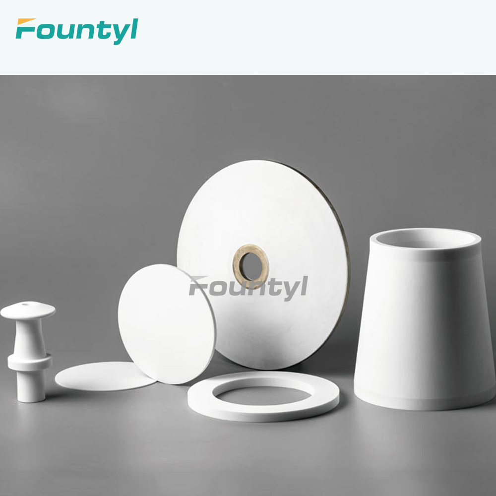
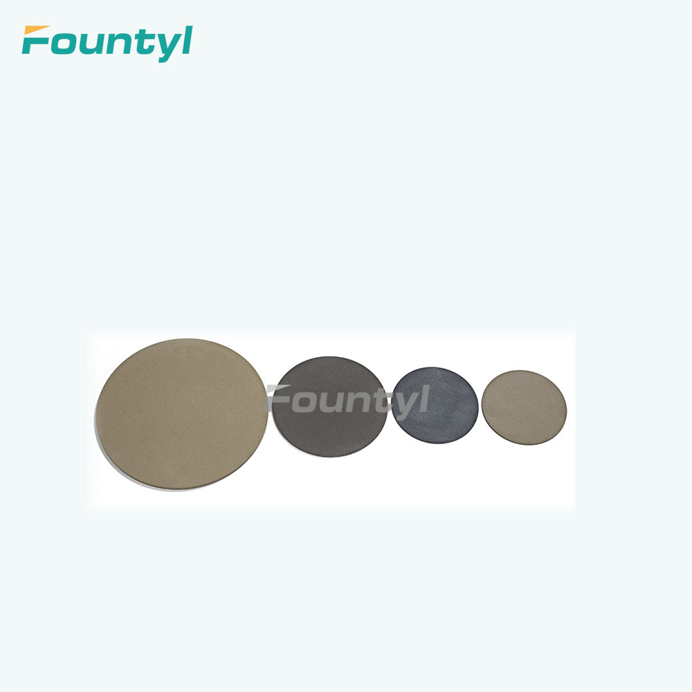
Material: Aluminum oxide ceramic or silicon carbide can be selected, and DLC and Teflon can be plated on the
surface.
High-precision SiC/SSiC wafer pin chucks are being developed for wafer exposure, inspection, transportation
processes that are highly flexible, very flat, and extremely resistant to harsh working environments.
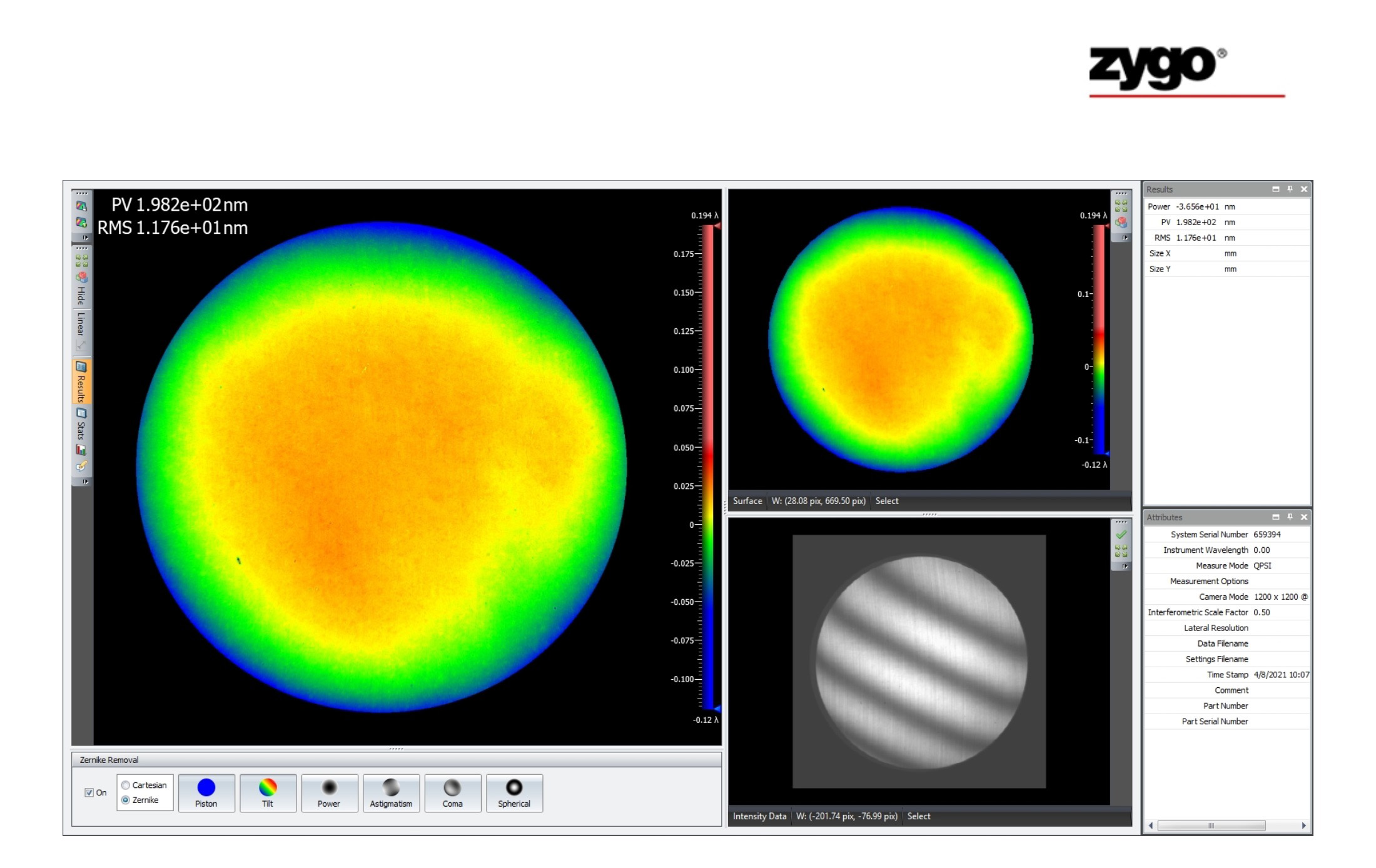
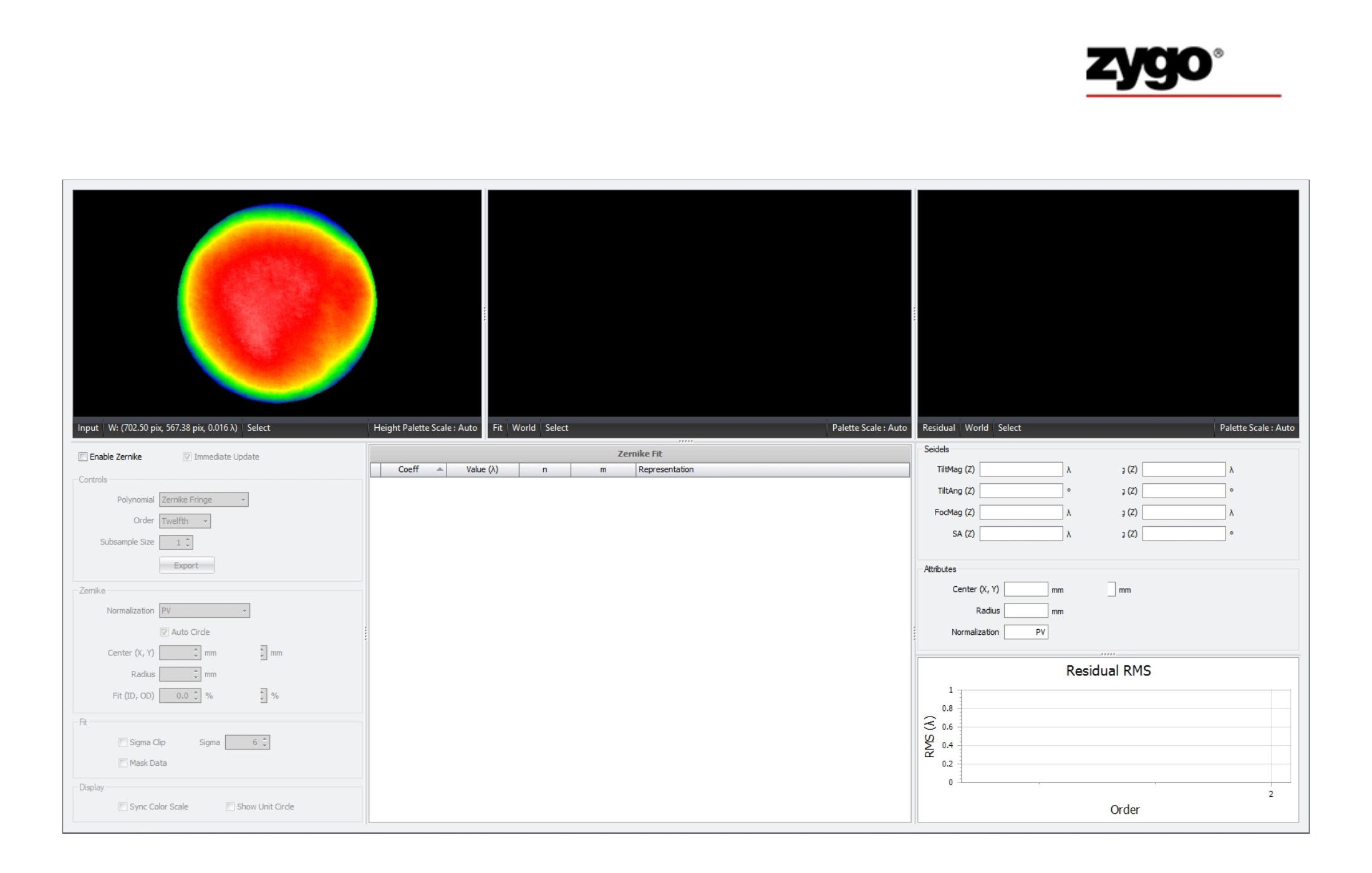
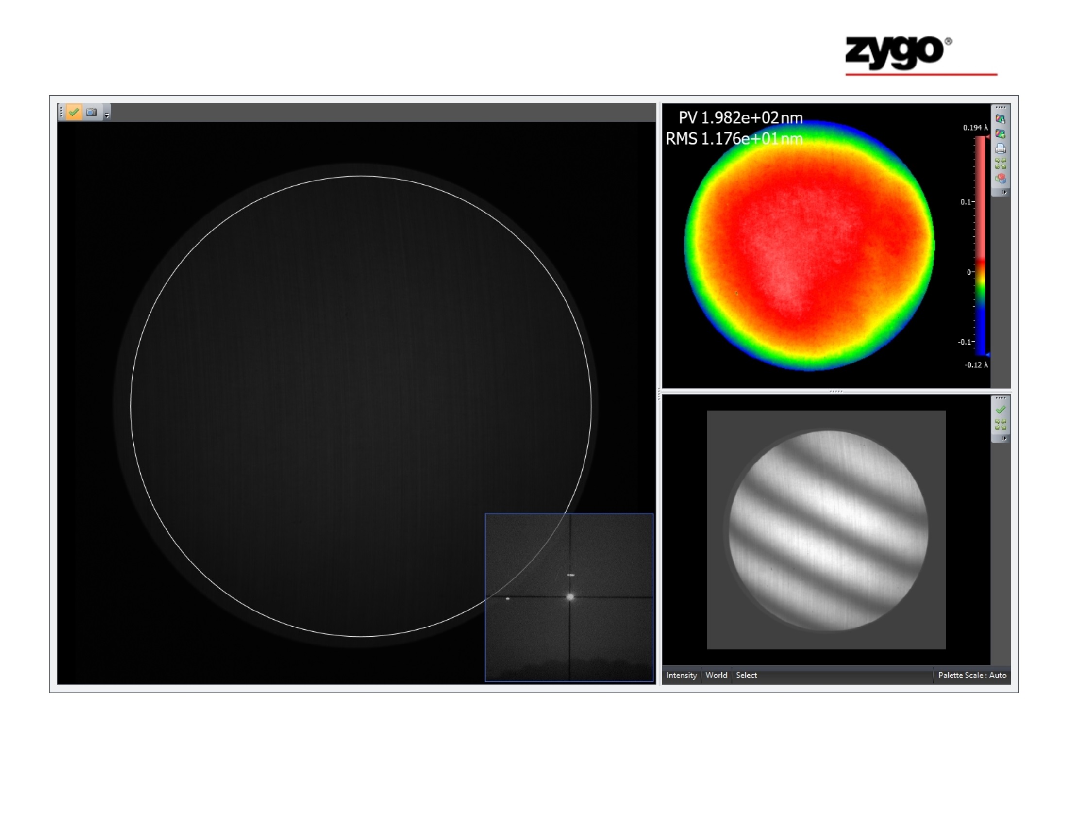
Precision Test Data
Application
Wafer fixation of semiconductor exposure device; Wafer fixation of wafer inspection device.