


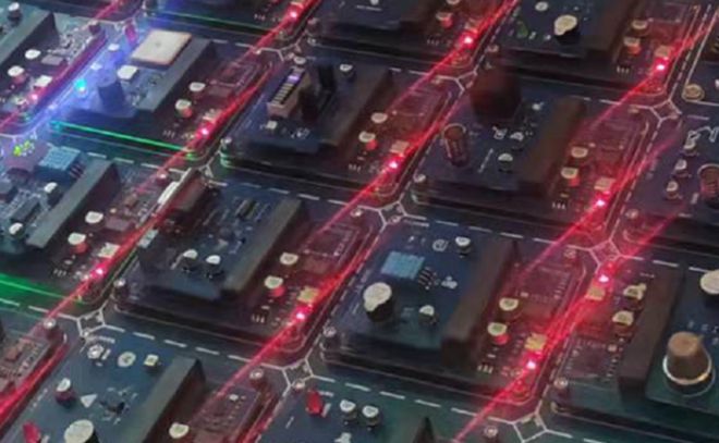
News

Chip bonding: The process of placing a chip on a substrate
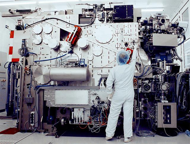
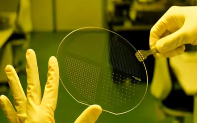
The packaging process is the last step in the manufacturing of semiconductors, and its sequence is grinding, cutting, mounting, wiring, and forming. The sequence of these processes can change according to the changes in packaging technology, and can also be closely related to each other or combined. This article focuses on wafer bonding, which is an encapsulation technique used to engage a chip separated from a wafer to an encapsulation substrate (lead frame or PCB) after a cutting process.
1. What is bonding?
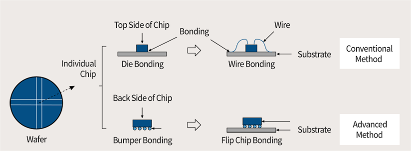
In the semiconductor process, "bonding" refers to the connection of a wafer chip to a substrate. Bonding can be divided into two types, namely the traditional method and the advanced method. Traditional methods include chip connections (or chip connections) and wire connections, while advanced methods include flip chip connections developed by IBM in the late 1960s. Flip chip bonding is a method that combines die bonding and wire bonding, and connects the chip and substrate by forming a convex on the chip liner.
2. Bonding process
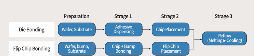
For chip bonding, the first thing to do is to coat the adhesive on the package substrate. Then, put a chip on it, pin side up. Instead, in the case of flip chip bonding, which is a more advanced method, small bumps called solder balls are attached to the liner of the chip. Then, the chip is placed on the substrate with the pin side down. In both methods, the assembled unit passes through a channel of temperature reflux that can be adjusted over time to melt the adhesive or solder ball. It is then cooled to attach the chip (or bump) to the substrate.
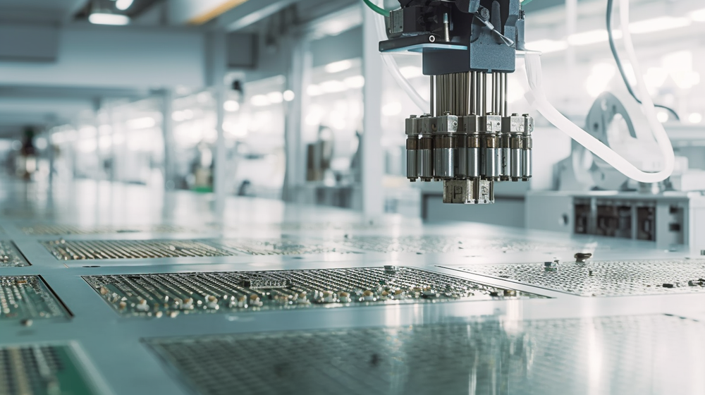
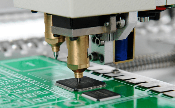
3. Pick & Place of Chips
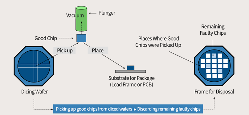
Removing the chip attached to the tape individually is called a "Pick." When the good chips are removed from the wafer with the plunger, placing them on the surface of the package substrate is called "Place". These two tasks, called "Pick & Place," are done on a Die Bonde.
4. Chip ejection
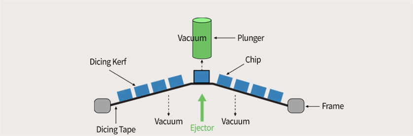
Use a method that is easy to pick up the chip: "ejection." An ejector is used to apply physical forces to the target chip, causing it to differ slightly in step size from other chips. After ejecting the chip from the bottom, pull the chip up from above with a vacuum band plunger. At the same time, pull the bottom of the tape with a vacuum to make the tape surface smooth.
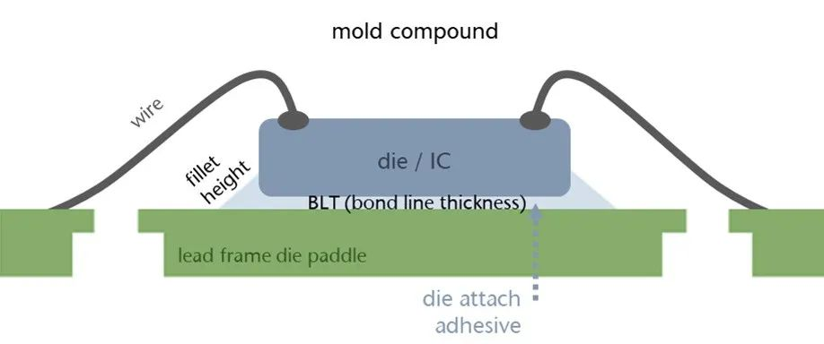
5. The chips are bonded with epoxy resin
When bonding the chip, the connection is made by using solder or paste containing metal (Power Tr), or polymer (polyimide) can also be used for chip bonding. In polymer materials, paste or liquid epoxy resins containing silver are relatively easy to use and have a high frequency of use.
6. Die coating (DAF) was used for chip bonding
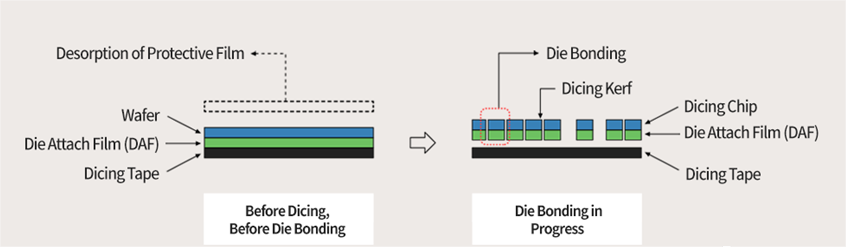
DAF is a thin film attached to the bottom of the chip. The thickness of the DAF can be adjusted to a very thin and constant thickness. It is widely used not only in chip-to-substrate bonding, but also in chip-to-chip bonding to create multi-chip packages (MCP). From the structure of the chip, the DAF at the bottom of the chip is glued to the chip, and the slicing tape is glued to the DAF below it, and the adhesion is weak. In order to perform chip bonding in this structure, after the chip and DAF are removed from the tape, the chip is placed directly on the substrate without the use of epoxy resin
Fountyl Technologies PTE Ltd, is focusing on semiconductor manufacturing industry, main products include: Pin chuck, porous ceramic chuck, ceramic end effector, ceramic square beam, ceramic spindle, welcome to contact and negotiation!