


News
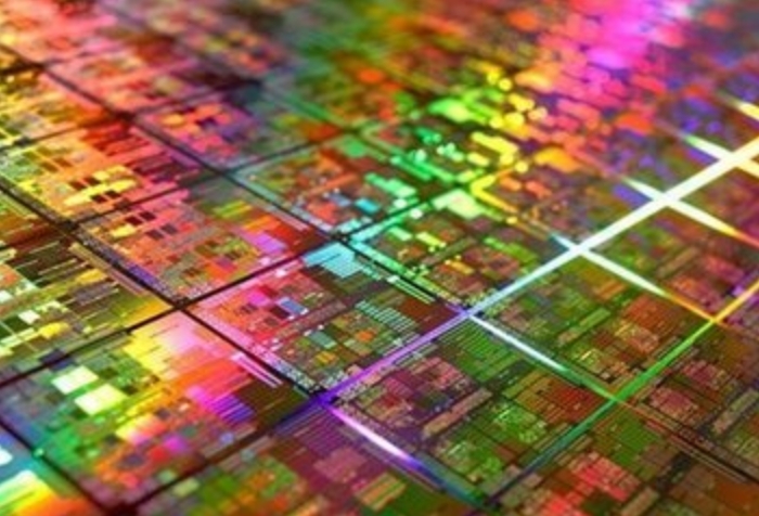
Common wafer development methods
The wafer development process is an essential step in the lithography process and has undergone decades of innovation and advancement. So how many common development methods are there? What are the types of developer? What is the development mechanism? What are the main controlling factors for development?
What is development?
photoresist development (photoresist development) is the application of a developer solution to a photoresist after exposure. The developer is a chemical solvent that washes away the exposed or unexposed part of the photoresist to get the desired pattern on the wafer. Specifically: In positive glue, the exposure part is washed away during development. In negative glue, the unexposed part is washed away during development.
Development mechanism of developer
Positive rubber
When the positive adhesive is exposed, the photochemical reaction of the photosensitive group will generate an acidic group, release nitrogen, and the acidic group will react with the developer, and the structure of the photoresist will be destroyed, so the photoresist after exposure will be washed away. Because the photoresist after exposure contains many acidic groups, the developer is generally a slightly alkaline solution.
Negative gum
When the negative adhesive is exposed, due to the reaction of the photosensitive groups, the polymer molecules in the photoresist will be cross-linked into a network structure, making the exposed photoresist structurally more stable and less soluble. The developer dissolves the unexposed (uncrosslinked) photoresist, while the photoresist in the exposed area remains unchanged.
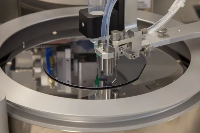
Common development methods
Immersion development:
Operation: In immersion development, the wafer is completely immersed in the developer for a fixed period of time. Pros: The process is simple. A uniform development is achieved because the entire wafer is evenly covered by the developer. It is commonly used in laboratory and research environments because it is easy to implement and does not require complex equipment.
Disadvantages: Not suitable for mass production, because a large amount of developer is required. The developer may be contaminated, especially if multiple wafers are developed consecutively. Control factors: temperature, time, concentration, developer fluidity. The same developer, the higher the temperature, the greater the concentration, the more intense the stirring, the faster the development rate.
Spray development:
Operation: Spray development uses specialized equipment to spray the developer evenly onto the wafer surface in the form of atomization. Advantages: High efficiency and developer savings. Because only the required amount of developer is sprayed onto the wafer, there is little waste. It can provide a very uniform development effect, and the wafer is sprayed and turned while developing. It is more suitable for mass production because it can process multiple wafers quickly and continuously.
Disadvantages: More complex equipment and more refined process parameter control are required to ensure that the spray is uniform. If the spray is not uniform, it may lead to inconsistent development results. Control factors: temperature, time, concentration, spray pressure, flow rate, wafer speed, etc.
Developer type
Positive developer: TMAH, NaOH, AZ 400K, AZ 826 MIF, AZ ECI 3027
Equinegative photoresist: AZ 326 MIF Developer, AZ 726 MIF Developer, AZ 826 MIF Developer, etc.
The above list is only the common developer, generally according to different photoresist, different resolution, different adhesive thickness to choose the appropriate developer.
Fountyl Technologies PTE Ltd, is focusing on semiconductor manufacturing industry, main products include: Pin chuck, porous ceramic chuck, ceramic end effector, ceramic square beam, ceramic spindle, welcome to contact and negotiation!