


News
Semiconductor process and equipment: etching process and equipment
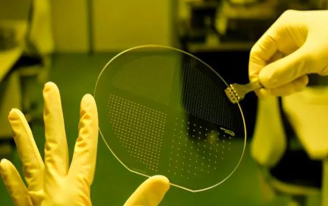
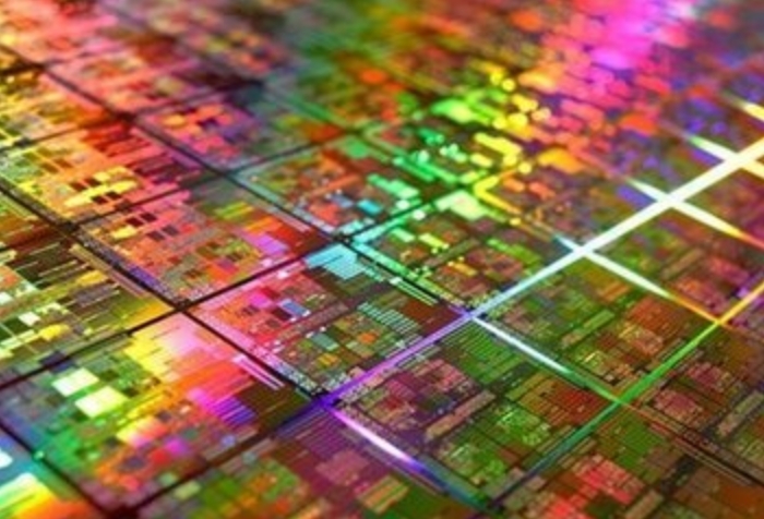
After the circuit diagram is lithographed on the wafer, an etching process is used to remove the excess oxide film, leaving the semiconductor circuit diagram. Etching, usually using chemical solutions, gases (or/and) plasma to remove selected excess material. the advantage of etching is that the sample making cost is low, and almost all commonly used industrial metal materials can be etched. There is no limit to the hardness of metal. Fast, simple and efficient in design.
There are two main methods of etching, depending on the substance used: using a specific chemical solution to proceed a chemical reaction to remove the wet etching of the oxide film and dry etching which uses gas (or/and) plasma, Dry etching technology is divided into reactive ion etching (RIE), sputtering etching and gas phase etching. below we describe the process and equipment of each etching method in detail:
I, Wet etching process
Using chemical solutions to remove the wet etching of oxide film, which has the advantages of low cost, fast etching speed and high productivity. However, wet etching is isotropic in that its velocity is the same in all directions. This results in the mask (or sensitive film) not being perfectly aligned with the etched oxide film, so it is difficult to handle very fine circuit diagrams.
The advantage of wet etching is that it is low cost and can be mass-produced. and can etch many pieces of wafer at the same time. So wet etching still plays an important role in the cleaning of large MES devices and non-critical layers. In particular, it is more effective and economical than dry etching especially in the etching of oxide removal residues and skin stripping.
·The main objects of wet etching are silicon oxide, silicon nitride, monocrystalline silicon and polycrystalline silicon. Hydrofluoric acid (HF) is usually used as the main chemical carrier for wet etching of silicon oxide. In order to improve selectivity, dilute hydrofluoric acid buffered by ammonium fluoride is used in the process. In order to keep the pH stable, a small amount of strong acids or other elements can be added. Doped silicon oxide corrodes more easily than pure silicon oxide. Wet chemical stripping is mainly used to remove the photoresist and hard mask (silicon nitride). heat stable alkaline phosphatase(H3PO4) is the main chemical liquid used for wet chemical stripping to remove silicon nitride, and has a better selection ratio for silicon oxide.
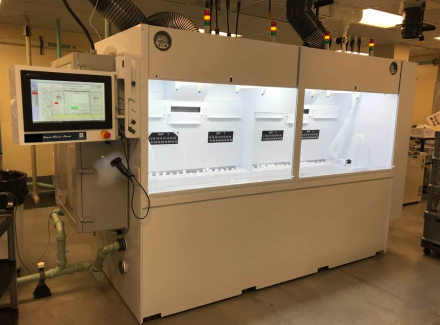
II, Wet etching equipment
Wet process equipment can be divided into three categories:
1,wafer cleaning equipment, the cleaning target objects include particles, organic matter, natural oxide layer, metal impurities of pollutants;
2,wafer brushing equipment, the main purpose of which is to remove the wafer surface particles;
3,wafer etching equipment, which is mainly used to remove thin films. According to the different uses of the process, the single wafer etching equipment can be divided into two types:
A) Light etching equipment, mainly used to remove the surface film damage caused by high-energy ion implantation;
B) Sacrificial layer removal device, which is mainly used for the removal of the barrier layer after wafer thinning or chemical mechanical polishing.
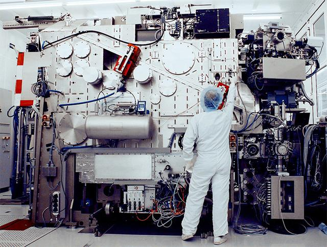
From the overall structure of the machine, the basic architecture of all kinds of wafer wet process equipment is similar, generally composed of the main frame, wafer transmission system, cavity module, chemical liquid supply transmission module, software system and electric control module 6 parts.
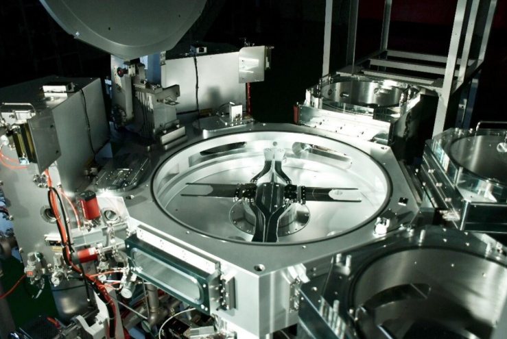
III, Dry etching
Dry etching because of its good directivity, gas ratio and RF power supply, it can also achieve more precise control, in the mainstream chip process, more than 90% of chip etching are dry method.
Dry etching can be divided into three different types: chemical etching, physical sputtering, and ion etching.
1, chemical etching: Chemical etching is a process that uses chemical reactions to remove the surface of a material. It uses etching gases (mainly hydrogen fluoride). Like wet etching, this method is also isotropic, which means it is also unsuitable for fine etching.
2, Physical sputtering etching
Physical etching is the use of glow discharge to ionize a gas, such as Ar gas, into positively charged ions, and then bias to accelerate the ions, splash on the surface of the etched object, and the etched atom is hit, sputtered, the process is completely physical energy transfer.
Physical sputtering has very good directivity and can obtain a nearly vertical etching profile. However, because the ions are fully and uniformly sputtered on the chip, the photoresist and the etched material are etched at the same time, resulting in a poor etching selection ratio. At the same time, most of the substances knocked out are non-volatile substances, which are easy to be deposited on the surface and side walls of the etched film. Therefore, in the manufacture process of VLSI, completely physical dry etching methods are rarely used.
3, RIE:Reactive Ion Etching
RIE combines the first two methods, that is, using plasma for ionizing physical etching, while using the free radicals generated after plasma activation for chemical etching. In addition to etching faster than the previous two methods, RIE can use the characteristics of ionic anisotropy to achieve high precision pattern etching.
4, Dry etching equipment
According to the material to be etched, etching is mainly divided into silicon etching, medium etching and metal etching.
There is a large gap between the etching machines used for different etching materials. The plasma generation methods of dry etching etchers include CCP (capacitive coupling) and ICP (inductive coupling). Due to the different technical characteristics of different ways, they are also distinguished in the downstream application fields. CCP technology has high energy but poor adjustability, which is suitable for etching hard dielectric materials (including metals); ICP low energy but strong controllability, suitable for etching monocrystalline silicon, polysilicon of low hardness or thin materials.
There are relatively few participants in the global etching machine equipment, and the industry as a whole is in an oligopoly pattern. Major players include Lam Research (Pan-Forest Semiconductor), AMAT (Applied Materials) in the United States, and TEL (Tokyo Electronics) in Japan. These three companies account for 94% of the global market share of semiconductor etchers, while the other players together account for only 6%. Among them, Lam Research accounts for as high as 55%, which is the absolute leader of the industry. Tokyo Electronics and applied Materials accounted for 20% and 19%, respectively.
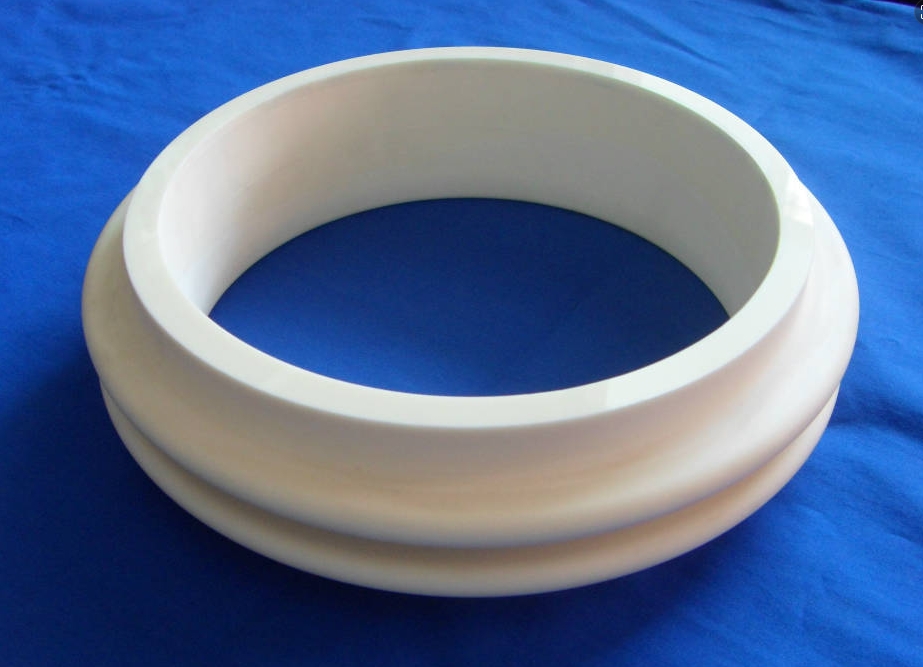
From the perspective of the domestic etching machine market, Lam Research still occupies a stable leading position. and we can also see that some domestic etching machines are growing and rising. Fountyl Technologies PTE Ltd, is focusing on semiconductor manufacturing industry, main products include: Pin chuck, porous ceramic chuck, ceramic end effector, ceramic square beam, ceramic spindle, welcome to contact and negotiation!