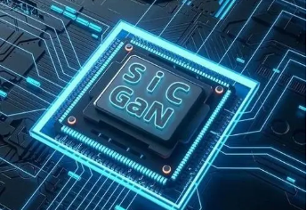
News
Silicon carbide wafer cutting types
Silicon carbide is a very hard and brittle material (Mohs hardness 9.2), which can cause processing problems. This is especially true during the back-end process, where wafers must be splited into separated chips before being packaged.
1,Diamond blade cutting
Mechanical diamond blade cutting is a traditional technique for separating SiC wafers.
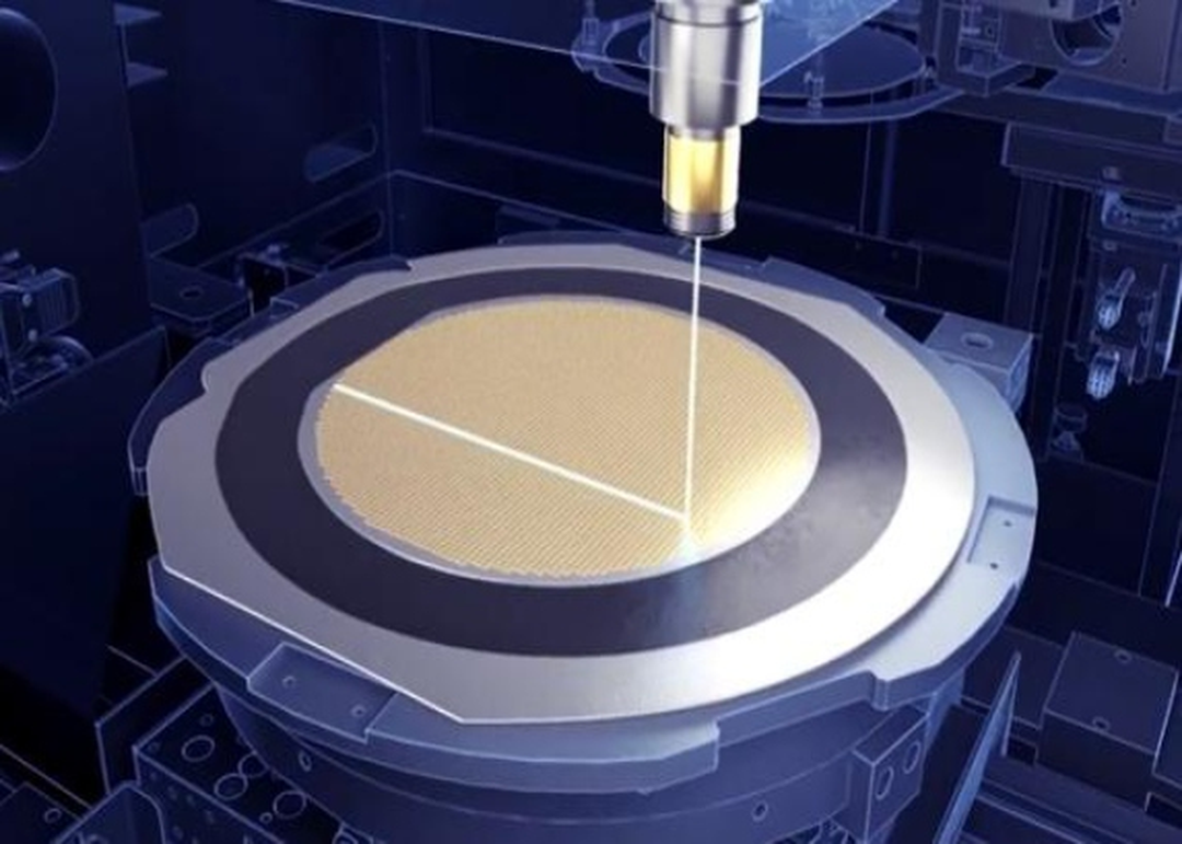
The wafer is mounted on a blue film and cut by a diamond-coated blade that rotates at high speed. The width of the cutting runway is usually in the range of 50 to 100 microns.
Due to the hardness of SiC, the cutting speed of blade is lower, and the abrasion of the cutting blade is higher, resulting in higher costs. In addition, blade cutting can cause chip edge fragmentation and delamination. with the silicon carbide wafer size changed from 4 inches to 6 inches in diameter, the cumulative runway length more than doubled, beyond the ability of a standard blade to do all the cutting. As a result, the blade must be replaced while the wafer is still in the working position and can rupture during the cutting process, damaging the wafer.
For example, one pc of SiC wafer scribing in 100mm (4-inch) needs to take 6 to 8 hours, and it is easy to cause edge breakage. Therefore, this traditional inefficient processing method has been gradually replaced by laser scribing.
2,Laser ablation cutting
Laser ablation is an alternative to mechanical wafer cutting. The laser beam is focused on the cutting runway. The material is heated by the absorbed laser energy. This results in significant heat-affected areas and micro-cracks. The blue film may also be affected by heat, which may affect the subsequent packaging process. In addition, the ablation rate is very low and needs to be performed several times to separate the chip. The number of repetitions depends on wafer thickness and cutting speed. In order to avoid material residue on the chip, the surface of the wafer must be coated with a protective coating. The main disadvantages of this cutting technology are low edge quality and low productivity.
In stealth cutting, a short-wavelength laser beam passing through a SiC wafer is focused inside the material. It creates a layer of localized defects inside the material, which becomes the starting point for wafer separation. First, the laser beam is focused on the lower part of the wafer and moves up layer by layer. Due to the split process, there is no material removal in the cutting path, resulting in zero incision. Second, the final separation of the chip must be accomplished by a separate mechanical splicing process as well as the expansion of the blue film. Because the laser heats the material inside the wafer, there is no thermal damage to the wafer surface. Defects in the pearl necklace pattern with overlapping areas can be only arised inside the material. In addition, each cutting rate is about 200mm/s, and in some applications can reach 300mm/s. However, depending on the thickness of the material, the laser needs to go through several times before it is able to separate the chip. This results in damage to the side walls of the chip due to the altered layer. In order to focus the laser beam on very small points inside the wafer, the beam scattered on a flat surface in the cutting runway needs to be smooth and minimized. In order to avoid the reflection of the laser, a metal cut-free runway is required. Another disadvantage is that the width required to open the runway is a function of wafer thickness (typically 40% of wafer thickness), which means that for a standard SiC wafer with a thickness of 350μm, the necessary minimum cut runway width is 140μm.
3, TLS cutting
Thermal Laser Separation is a fast, clean and cost-effective alternative to separating silicon carbide wafers. The laser heats the material and creates a region of compressive stress surrounded by a pattern of tangential tensile stress. Then a very small amount of deionized water spray is sprayed, which creates a second cooled zone near the first zone, causing a pattern of tangential tensile stress. Tensile stress is created in the region where the two stress patterns overlap, which opens and guides the crack tip through the entire material.
TLS cutting is a single-step process that can separate wafers of the entire thickness at separation speeds of up to 300mm/s. The starting point is a local or continuous shallow scratch on the wafer surface. Since TLS cutting is a split process, it has the potential to reduce the width of the cutting runway and increase the number of chips on each wafer. The edge of the chip is smooth, without residual stress or micro-cracks and fragmentation zones. The metal structure (PCM) on the front runway and the polyimide on the chip are acceptable. In addition, since the separation is derived from the lobe rather than the subsequent physical separation/fracture, the backing metal can be separated without delamination or being affected by heat. Yield analysis using the TLS cutting process on a typical power device wafer with a fully metallized back shows that the average yield of polyimide and metal structures on the cutting runway exceeds 98%.
4,Water guided laser scribing
The water guide laser is to focus the laser into the micro-water column, the diameter of the water column varies according to the nozzle aperture, there are 100 ~ 30 μm various specifications. Using the principle of total reflection between the water column and the air interface, the laser will be propagated along the direction of water column travel after being introduced into the water column. It can be processed within the stable range of the water column, and the overlong effective working distance is especially suitable for the cutting of thick materials. When traditional laser cutting, the accumulation and conduction of energy is the main cause of thermal damage on both sides of the cutting path, and the water-guided laser will quickly take away the residual heat of each pulse because of the role of the water column, and will not accumulate on the workpiece, so the cutting path is clean. Based on these advantages, in theory of water-guided laser cutting silicon carbide is a good choice, but the technology is difficult, the relevant equipment maturity is not high, as a wearing part of the nozzle with big production difficulty, if you can not accurately and stably control the tiny water column, splashing water droplets ablation the chip, affecting the yield. Therefore, the process has not yet been applied to the production of silicon carbide wafers.
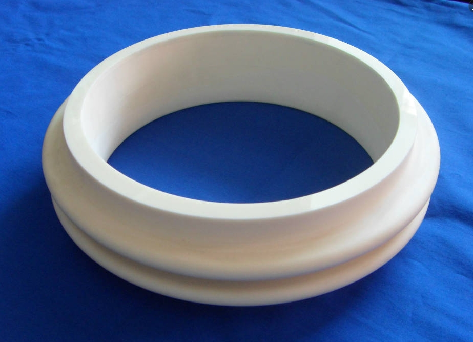
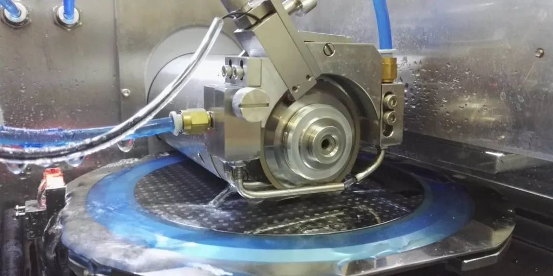
Fountyl Technologies PTE Ltd is specializing in ceramic vacuum chuck, provides the best ceramic fixture for SIC cutting process, various chucks in 2/3/6/8/12/14 inch.