


News


ASML's entrepreneurial Story: The Path to Growth for a lithography giant
ASML was founded on April 1, 1984 as ASM Lithography. The mission of this joint venture between Philips and ASM International is to commercialize the PAS 2000, a wafer stepper developed by Philips.
1,Demultiplex of industry
In the 1960s and 1970s, chip makers built the vast majority of the semiconductor value chain in-house - all the steps needed to make a finished microchip. Then, in the late 1970s and early 1980s, semiconductor manufacturing technology grew rapidly in size and complexity. This development has driven the division of Labour in the semiconductor value chain. The semiconductor equipment industry emerged to provide off-the-shelf top end solutions. With this off-the-shelf capability, it no longer makes sense for chipmakers and users to develop their own chip-making equipment.
Specialist equipment suppliers are particularly important for developing complex lithography systems for printing patterns on microchips. Improving these systems so that they can print smaller features is key to advancing Moore's Law. For chip makers, more transistors means to obtain the more computing ability at a lower cost.
2,The prototype of PAS 2000
It was in this context that Philips began to develop its own wafer stepper for patterning silicon wafers. Prototypes Silicon Repeater (SIRE) I and II were developed by Philips Research Center. The Philips Automated Stepper 2000 was born from these research prototypes.
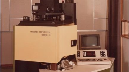
At the Philips Research Center, where Philips's division focuses primarily on basic research, wafer steppers are something of an anomaly. Market demand is increasingly driving enterprise research and development, and the engineering manufacturing equipment is used more. Start from 1978, Philips Science & Industry (S&I) promoted commercialization efforts under the name PAS2000.
3,Industrial policy, investors and entrepreneurs
Beginning in the late 1970s, under the direction of the European Commission, Western European governments reshaped industrial policy. They focus on innovation and collaboration, targeting emerging industries, particularly the rapidly growing semiconductor and microelectronics industries. These policies are new means of boosting economic activity and, if possible, reviving struggling conglomerates, many of which (including Philips) have begun to fall apart.
At the commission's request, Philips and other companies expressed the importance of these industries to their respective governments. After receiving this information from Europe's largest electronics company, the Dutch government has further understanding of the subject and informed their follow-up action.
Rising costs, global competition and technological advances are forcing large companies to divest non-core businesses and refocus their operations. For Philips, one of those activities was their wafer stepper. At the same time, emerging venture capital firms and entrepreneurial-driven start-ups and scale enterprises provide a new paradigm for industrial growth.
4,Pressure to make progress
In early 1982, Philips' lithography ambitions faced a major challenge. They need more engineering resources. Although they approached IBM, an external customer for the evaluation tool, there was considerable uncertainty about whether it would be delivered in time for the summer of 1982. Engineers at the Philips Research Center immediately came to the rescue. S&I executives frequently visit The Hague and Brussels to seek additional funding from the Dutch government and the European Commission. Under pressure from time, money and the Dutch Ministry of Economy, Philips S&I began looking for a partner for its wafer stepper. This led to initial discussions with Cobilt, a company that manufactures mask aligners and tracks, followed by discussions with lithography market leader Perkin Elmer.
At the same time, a three-way dialogue began between the Dutch Ministry of Economic Affairs, Philips and a growing Dutch company, ASM International (or ASM for short). In the context of the European Commission's novel microelectronics project ESPRIT, chip companies have expressed concern about their reliance on American equipment. To meet industry needs, the ministry and Arthur Del Prado himself proposed ASM as a potential solution.
5,Seeking partnerships
However, Philips considered ASM's position too low and favored Perkin Elmer. Despite Del Prado have entrepreneurial spirit and success, Philips executives still see ASM as an upstart. Perkin Elmer is a large and diversified company with a large installation base of lithography tools, was considered a stronger partner. The interest is mutual. By the early 1980s, wafer steppers provided more control over the smallest feature sizes with acceptable productivity than Perkin Elmer's Micraligns. The US company has sought to quickly consolidate its market position amid increased competition.
Perkin Elmer is considering partnering with Philips S&I or Liechtenstein-based startup Censor. They preferred Philips, citing the company's resources and the advanced nature of PAS 2000. In the proposed joint venture, Perkin Elmer will play a leading role and be responsible for sales and service. Philips will contribute technology and manufacturing capabilities. However, Philips hesitated to grant access to its internal resources, such as the subordinated Philips Research Center. This hesitation made the negotiations too long, and eventually Perkin Elmer teamed up with Censor.
6,Project urgency
By 1983, Philips S&I's wafer stepper team, consisting of about 50 engineers, was facing uncertainty. They will need around 120 million guilders (around 245 million euros at current pricing levels) to upgrade, produce and sell the machine. Despite Troost's strenuous and persistent efforts, including exploring partnerships with Varian and Panasonic, the wafer Stepper team was too late. The urgency is palpable.
7,Beginning of ASML
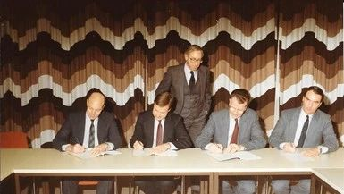
On 5 September 1983, Philips and ASM announced their intention to form a joint venture. Over the next few months, they refined the details of the partnership. Shares of the Ministry of Economy or its investment vehicles were considered. Negotiations were held to enter the Philips Research Center. Contributions in kind and in cash were specified. A return on investment plan was drafted. An ambitious and visionary new general manager, Gjalt Smit, took over. Importantly, the 50 existing Philips S&I employees have been offered attractive employment terms. But because they have worked at Philips all their lives, they see the joint venture as a form of divestiture for Philips. People are reluctant to put their faith in a start-up that has no market access and whose key technologies must be redesigned. in spite of this, the group still has 47 signatories.
From the beginning, ASML was seen as the embodiment of innovation-driven entrepreneurship and was expected to secure the future economic capacity of the Netherlands. Young companies, with impulse and enthusiasm, embark on an uncertain but hopeful future. Moving to Veldhoven may be the end of this story, but for ASML it's just the beginning. Those early days in the outside shed of Philips laid the foundation for ASML to grow into the company we know today. The team is creative and determined to pursue technological innovation and push the limits of what is possible.
8,Humble beginnings
In 1988, after Philips established a joint venture foundry in Taiwan, we began to enter the Asian market. In the United States, we have grown from a few employees to 84 across five locations. But in a highly competitive market with many suppliers, this little-known small company from the Netherlands could not break through.
ASML had too few customers to be self-reliant. To make matters worse, shareholder ASMI, unable to maintain a high level of investment with little return, decided to withdraw, while the global electronics industry situation went from bad to worse, Philips announced a massive cost-cutting program. The survival of our young, cash-gobbling lithography company hangs in the balance. Driven by a firm belief in ongoing research and development and an urgent need for funding guidance, ASML executives contacted Philips board member Henk Bodt, who convinced his colleague to lend a final hand.
9,From giving a hand to initial public offerings
The investment has been put to good use. During the year, we launched our breakthrough platform PAS 5500. With its industry-leading productivity and resolution, the PAS 5500 has attracted the key customers ASML needs to become profitable. This is the first step towards maturity.
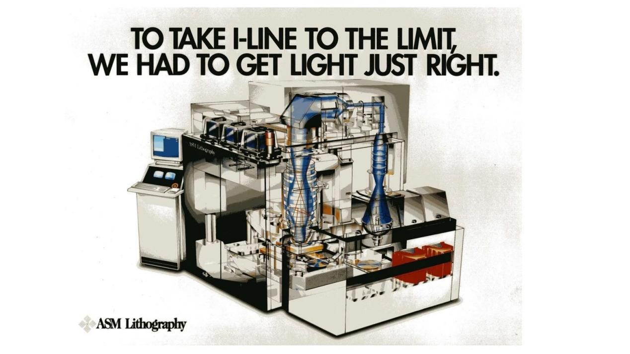
PAS 5500 is the platform for which ASML is known. Prior to its launch, ASML ranked third in the lithography market, behind giants Nikon and Canon. But the success of the PAS 5500 platform quickly propelled ASML to second place and set the stage for its growth as a global leader in lithography. The PAS 5500 grew out of a series of systems initiated by Philips researchers in the 1970s. The name of the platform itself reflects its heritage and our long-standing relationship with Philips: Philips Automatic Stepper (PAS).
ASML became a fully independent public company in 1995, listed on the Amsterdam and New York Stock Exchanges. Philips sold half of its shares in the initial public offering and the rest over the following years. The IPO brought in funds to further fuel our growth and we expanded our research and development and production facility in Veldhoven De Run, which later became our new headquarters.
10,TWINSCAN and immersion technology paved the way
In 2001, we introduced the TWINSCAN system and its revolutionary two-stage technology. These systems expose another wafer while measuring and aligning the next one, maximizing the productivity and accuracy of the system, thereby increasing the value of ownership for the customer. In the same year, we completed the acquisition of Silicon Valley Group, further enhancing ASML's capabilities in semiconductor technology advancements. The TWINSCAN AT:1150i debuted as the first immersion machine in 2003, followed by the TWINSCAN XT:1250i, XT:1400i, and the first mass-produced immersion machine, the XT:1700i, in 2006.
In 2007, we introduced the TWINSCAN XT:1900i immersion system with a numerical aperture of 1.35, the highest specification in the industry. With this new technology, we enable customers to produce smaller chip features by projecting light through the water layer between the lens and the wafer. Later in 2007, we acquired BRION, a leading provider of semiconductor design and manufacturing optimization solutions. This was the beginning of our "holistic lithography" strategy. We combine our knowledge of lithography systems with our skills in optimizing chip manufacturing processes before, during and after lithography. Another key product in the early stages of our overall lithography strategy is YieldStar, our metrology system that provides real-time measurement and calibration during the chip manufacturing process. The first YieldStar (250D) was delivered to customers in 2008.
11,Change The Times again with EUV
In early 2020, the EUV entered mass production and we celebrated the shipment of our 100th EUV system. But 2020 is also significant for another reason: the COVID-19 pandemic. Our teams around the world have proven their ability to adapt and improvise by supporting customers remotely in innovative new ways, using their expertise to respond to pandemics and reaching out to support local communities. prove that they have ability to adapt and improvise.
In November 2020, the acquisition of the Berliner Glas Group was completed and we officially welcomed the Berliner Glas team into the ASML family. The Group's technical Glass division was spun off to the Glas Trosch Group in April 2021.
In 2023, we introduced the first next-generation EUV system with a numerical aperture up to 0.55 (called "high numerical aperture"). The platform, called EXE, features a novel optical design and a significantly faster platform.
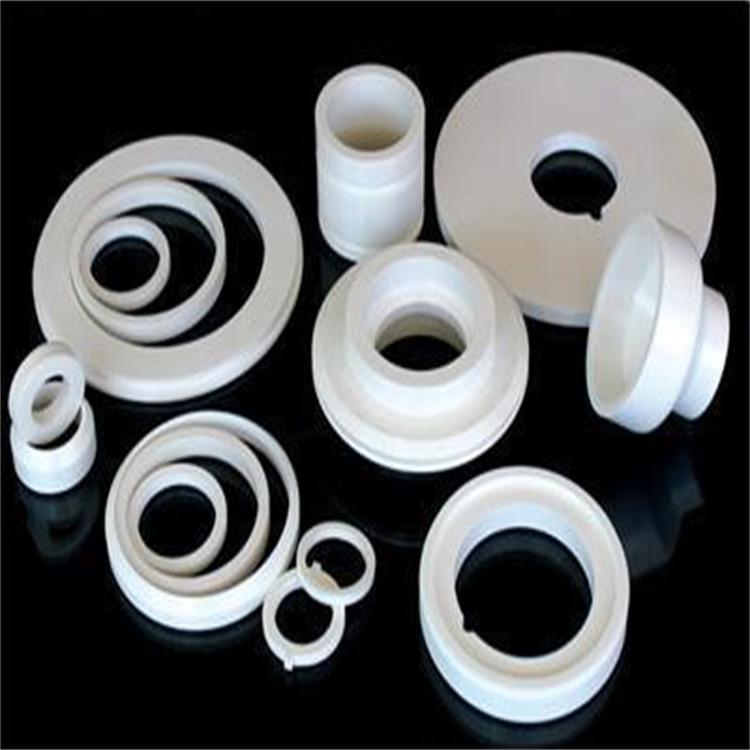
Looking ahead, ASML will continue to work wonders. Fountyl Technologies PTE Ltd, is focusing on semiconductor manufacturing industry, main products include: Pin chuck, porous ceramic chuck, ceramic end effector, ceramic square beam, ceramic spindle, welcome to contact and negotiation!