


News
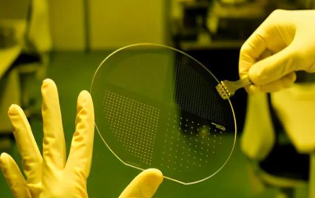


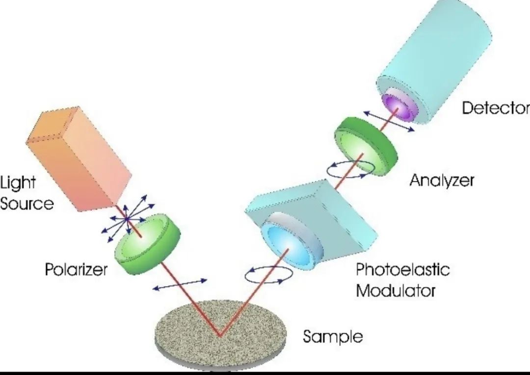
Confocal light microscope
The laser is focused on the wafer, illuminates a light spot, and the reflected light is refocused on the receiving plane, and through the analysis of the light, the surface of the silicon wafer is detected. The microscope is a system in which laser light is focused on a silicon chip and the reflected light is designed to be focused using a receiver. In other words, the defocusing information does not pass through the receiving plane and thus a high-resolution, high-contrast image can be obtained.
Of course, the resolution of light microscopes is limited, and there are also devices for monitoring using SEM.
Particle testing equipment
The particles on the silicon chip will directly lead to a decrease in the yield, for example, in advanced LSI, the LSI wiring size is tens of nanometers. If there are particles on the surface of the ghost film, it is easy to destroy the pattern when forming the wiring, so it is necessary to strictly control the surface particles.
Automated monitoring devices with wafer loading and unloading capabilities are the most common. The position of the particles is immediately displayed as an image.
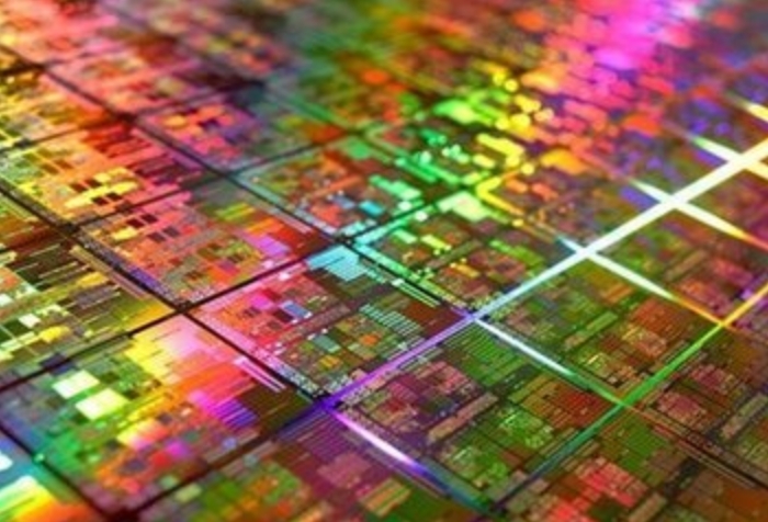
Defect detection equipment with patterned wafer
The patterns, particles and defects on the surface of patterned wafers have high requirements for S/N ratio and resolution.
Although the surface monitoring method with patterned wafers also uses light scattering method, the pattern contrast method is the mainstream technology. In this method, the wafer is illuminated with illumination light, the image is imprinted on the monitoring surface, and the obtained image signal is input to the computer, and the defect is monitored by comparing the image signals of the same pattern. In this way, the effects of underlying patterns and uneven shapes can be eliminated,
SEM for observing wafers
SEM stands for Scanning Electron Microscope. SEM is mainly positioned as an observation device. The presence of SEM is indispensable for promoting the refinement of the front process. SEM can observe the process results and improve the process conditions. SEM is also indispensable as a process monitor in the fabs field. The connection between the two is so close that the refinement of the semiconductor promotes the high-resolution SEM.
CD SEM
The fastest way to monitor lithography results is CD-SEM. Resolution pattern for day and night monitoring of photoresistance. This is of course non-destructive monitoring.
Monitoring the resolution of resist is an important on-line monitoring. In this process CD SEM is essential. Although SEM is now the mainstream method, but initially because the size of the pattern is not so small, the monitoring method of light microscopy is used. When the design size is close to 1μm, it is impossible to measure the resist pattern with the resolution of optical microscope, so the SEM method comes into being. In addition, the SEM has a focal length approximately 1000 times that of an optical microscope, with the ability to measure the length at the top and bottom of the resist pattern.
Overlay measuring equipment necessary for photolithography
Resolution is important in lithography, and overlay accuracy is equally important. This is because semiconductor processes use dozens of masks to form layered patterns.
Overlap is monitored by monitoring the overlap gap between the pre-formed marks on the product circle and the marks on the optical mask. These tags are called Ber in Bar and Box in Box, and the tags themselves are about 20um in size. These markers or masks are located at the four corners of each exposure mirror. The measurement of multiple exposure mirrors is carried out on a wafer, and the data is statistically processed and fed back to the exposure device.
Film thickness measuring equipment
There are approximately three categories of film thickness determination methods for semiconductor processes.
① Physical contact measurement.
② Optical measurement.
③ X-ray measurement.
The most common is optical measurement, which is a non-destructive and non-contact measurement method.
Other measuring equipment
Trends in microscopy
Since SEM is not suitable for observing four-convex surfaces, probe microscopes such as Scanning Tunnel microscopy (STM) or Atomic force microscopy (APM) have also become widely used. These devices scan the surface by tracking it with cantilevers and monitoring tunnel currents and atomic forces at the tip to measure the surface's subtle four-convex shape. These devices have high resolution but small measurement areas.
Other measuring equipment required in the process includes resistance measuring equipment and flatness measuring equipment. The former monitors the resistance value after ion injection and heat treatment to monitor and control doping results. The latter measures the flatness after the CMP.
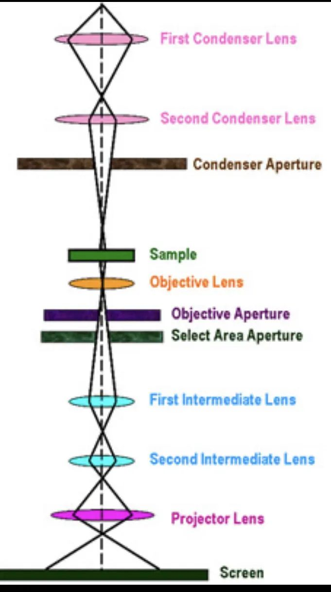
TEM
A transmission electron microscope (TEM) may be required to directly observe the defective part. FIB is a very powerful tool for preparing these observational samples. TEM stands for Transparent Eleetron Mieroscope (Transmission electron Microscope).
Improve the yield by testing equipment
The results of post-process monitoring/measurement are fed back to each process and this feedback mechanism helps to stabilize the process quality. In addition, particle-related monitoring results are fed back to the clean room to help better manage and maintain manufacturing equipment.
Compare using FMB
FBM stands for Fail Bit Map. After finishing the wafer process or removing the wafer in the middle, the display form of the area judged to be defective is measured by the detection equipment, and the defect map of the patterned wafer defect monitoring equipment can be compared to determine which defects are fatal defects.
In addition to defect analysis after the completion of the wafer process, this method is also used for real-time monitoring of the process. In this application scenario, the ability to quickly analyze newly discovered defects is important because it can help us identify early on whether a defect will become fatal and reverse it to the process management mechanism.
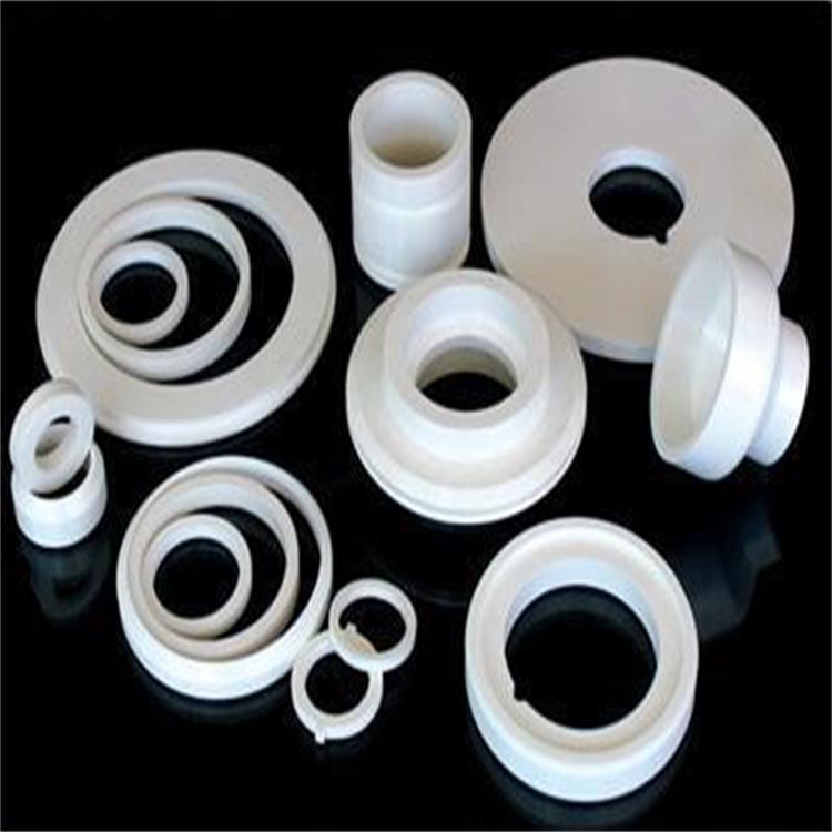
Fountyl Technologies PTE Ltd, is focusing on semiconductor manufacturing industry, main products include: Pin chuck, porous ceramic chuck, ceramic end effector, ceramic square beam, ceramic spindle, welcome to contact and negotiation!