


News


Introduction on application of semiconductor precision ceramics
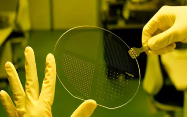
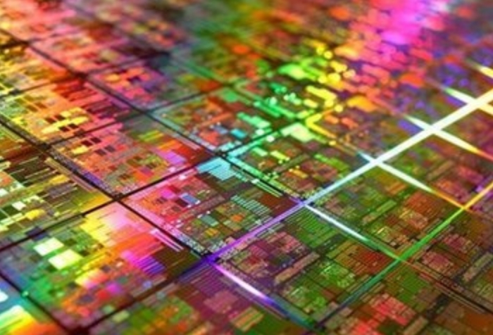
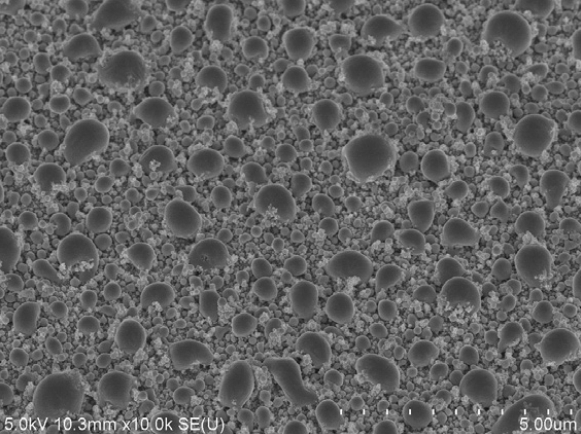
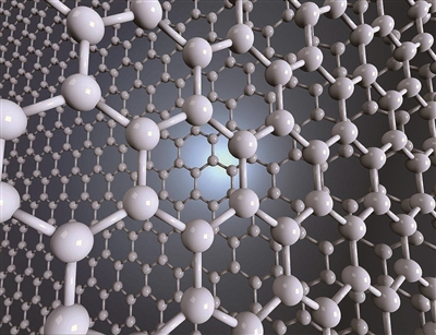
Advanced ceramics are the foundation of the entire semiconductor industry foundation. Because ceramics have the advantages of high hardness, high elastic modulus, high wear resistance, high insulation, corrosion resistance, low expansion...etc., it can be used as parts of silicon polishing machine, epitaxial/oxidation/diffusion heat treatment equipment, lithography machine, deposition equipment, semiconductor etching equipment, ion implantation machine. Semiconductor devices require a large number of precision ceramic components. Semiconductor equipment ceramics include alumina, zirconia, silicon nitride, aluminum nitride, silicon carbide, yttrium oxide...etc. In semiconductor equipment, the value of precision ceramics accounts for about 16%. Semiconductor equipment is the key support of the semiconductor industry chain and the cornerstone of semiconductor manufacturing, and the latest SEMI report predicts that global semiconductor equipment sales will be $87 billion in 2023 to $87.4 billion, and will be recovered to $100 billion in 2024.
With the vigorous development of the domestic semiconductor industry, wafer foundries have built factories in Southeast Asia, which has led to the improvement of semiconductor materials and equipment supporting, foreign supply chain resource allocation to the domestic tilt, but also the emergence of many excellent local semiconductor equipment manufacturers, under the trend of domestic development, the demand for semiconductor equipment precision ceramic parts will increase.
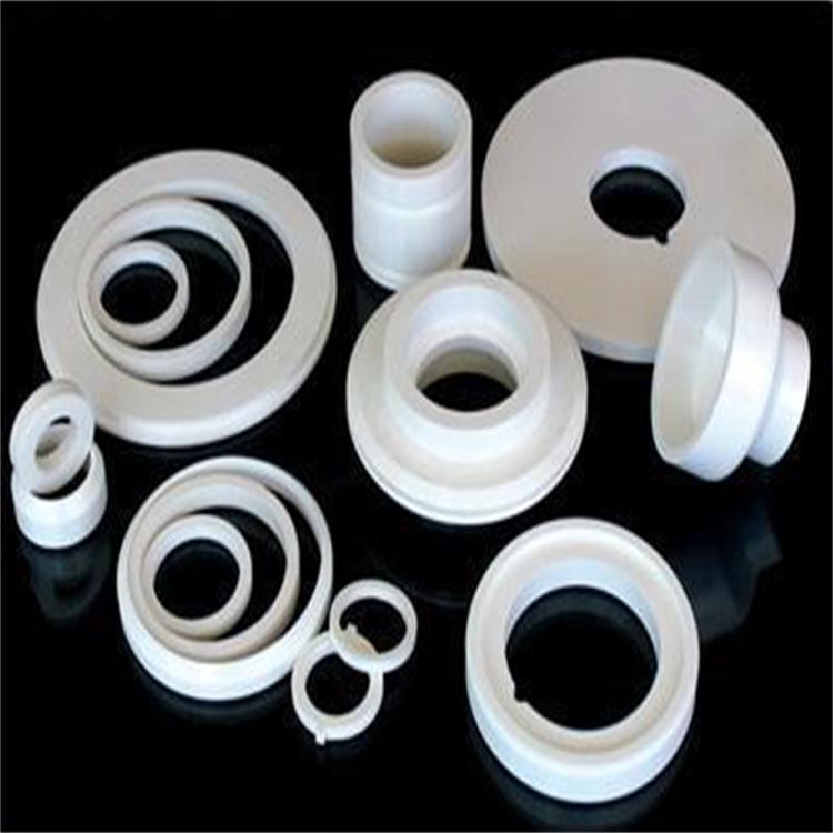
Because of its position and importance in semiconductor equipment, advanced ceramic parts must meet the comprehensive performance requirements of semiconductor equipment for materials in mechanical mechanics, heat, dielectric, acid and alkali resistance and plasma corrosion, and high precision requirements, because ceramic parts in semiconductor equipment are usually closely around the wafer, and some even directly contact the wafer. Therefore, the control of metal ions and particles on its surface is extremely strict. In addition, because the production of ceramic components for semiconductor devices involves original equipment manufacturer certification, Therefore, it belongs to the industry with high threshold of exclusivity, In addition, in the field of semiconductor packaging and testing, ceramic materials can also be used in power semiconductor device packaging liners and test probe cards.
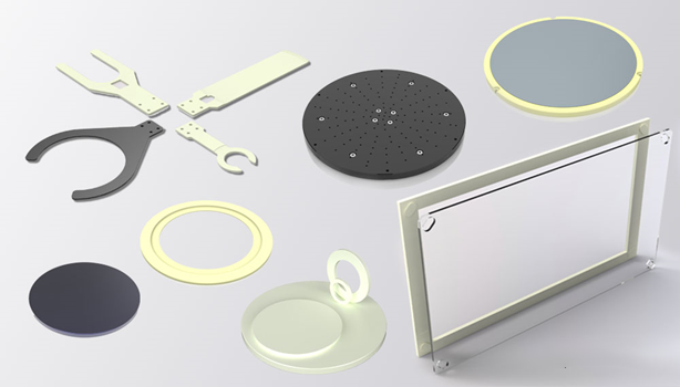
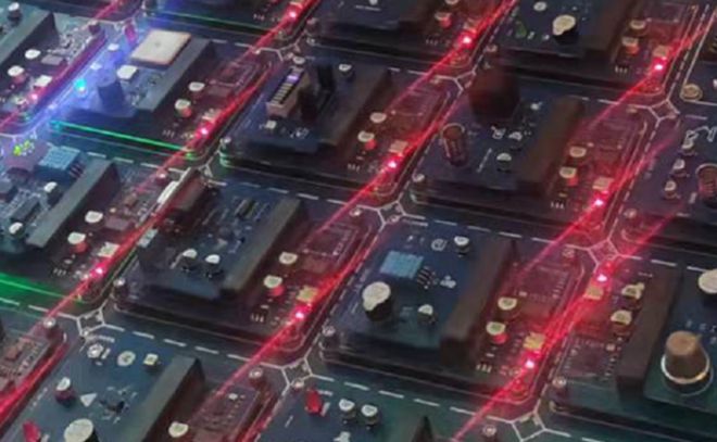
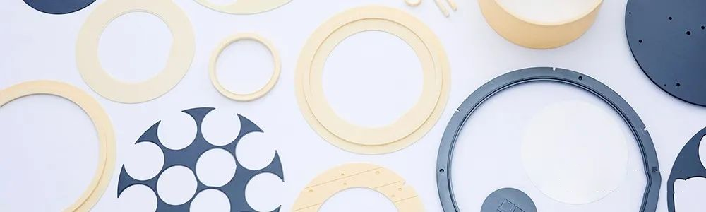
Semiconductor ceramic industry chain includes semiconductor wafer processing, power semiconductor devices, packaging and testing of downstream application enterprises; Lithography equipment, oxidation diffusion equipment, etching equipment, dry engraving equipment, ion implantation equipment, film deposition equipment, PVD equipment, CVD equipment, atomic layer deposition (ALD) equipment, chemical mechanical polishing equipment, laser annealing equipment of high-end semiconductor equipment enterprises; Powder preparation equipment, mixer, sanding machine, three-roll machine, spray granulation equipment, injection molding machine, casting machine, laminating equipment, dry pressing equipment, grouting molding, isostatic pressing equipment, screen printing equipment, defatting, sintering equipment, CNC, milling machine, polishing equipment, sandblasting equipment, vacuum brazing equipment, tooling fixture of production equipment and accessories enterprises; Ceramic parts (handling arm, electrostatic chuck, ceramic heater, lining ring, nozzle, chamber, probe card, ceramic splinter...etc.), alumina ceramics, porous ceramics, zirconia ceramics, aluminum nitride ceramics, silicon nitride ceramics, silicon carbide ceramics, aluminum silicon carbide ceramics...etc.