


News


Key component of semiconductors - Introduction of ceramic chuck and global market.
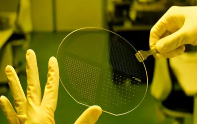
Electrostatic sucker , also known as electrostatic chuck (ESC, e-Chuck), is a fixture that uses the principle of electrostatic adsorption to hold and fix the adsorbed object, suitable for vacuum and plasma environment, the main function is used to adsorb ultra-clean sheet (such as silicon), and make the adsorb object to maintain a good flatness, can inhibit the deformation of the adsorb object in the process. and can adjust the temperature of the adsorb object.
Mechanical clamping: In the early silicon wafer processing, it is used to the mechanical clamping method in the traditional mechanical industry, that is, the clamp of mechanical activity is used to clamp the silicon wafer, but the clamp will cause damage to the edge of the silicon wafer, and it is easy to warp the silicon wafer, which has a great impact on its processing accuracy, so the mechanical clamping method is rarely used now.
Paraffin wax bonding method: Usually the silicon wafer is fixed on the characteristic position of the fixture first, and then the adhesive is infiltrated between the silicon wafer and the fixture by heating and melting, then to fix, In order to ensure the reliability of the binder and the fixed accuracy of the silicon wafer, it is necessary to melt and filter the binder before removing impurities. In the whole clamping process, the paraffin wax needs to be heated, bonded, stripped and cleaned, and the efficiency is very low. At the same time, the binder will have a greater impact on the cleanliness of the silicon wafer, and it is difficult to ensure the uniformity of the paraffin bond layer and ensure no bubbles.
Vacuum chuck: The working structure of the vacuum chuck is mainly divided into two parts, the middle part is porous ceramic, and the edge part is a sealing ring. When working, the air between the silicon wafer and the ceramic surface is extracted by the small hole on the porous ceramic, so that the silicon wafer and the ceramic surface achieve low pressure, and the silicon wafer is adsorbed on the surface of the chuck due to the air pressure, thus fixing the silicon wafer. Wait until the end of the processing, the internal ionized water will flow out from the ceramic surface, and the ionized water can prevent the silicon wafer from adhering to the ceramic surface, and at the same time, the silicon wafer and the ceramic surface can be cleaned, and the chuck will continue to clamp the next piece of silicon after the cleaning is completed. vacuum chuck has two main disadvantages:
1, When the silicon wafer is adsorbed on the surface of the vacuum chuck, the silicon wafer will cause local deformation due to air pressure, and the silicon wafer will rebound after processing, resulting in its cut surface showing a corrugated shape, and the surface smoothness decreases. In addition, there may be small particles sucked between the silicon wafer and the chuck during processing, so that the local deformation of the silicon wafer affects the processing accuracy.
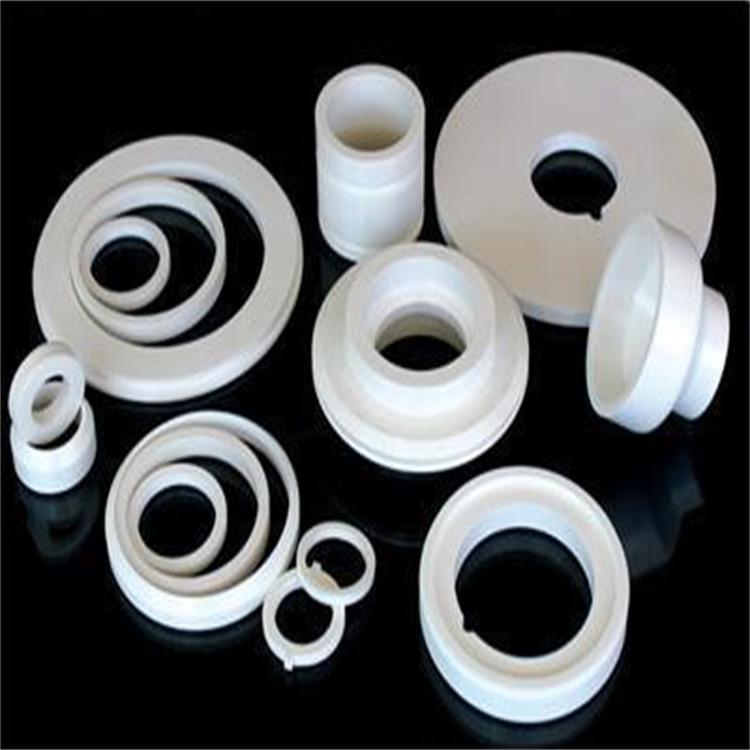
2, If the silicon wafer needs to be processed in a vacuum environment, the vacuum chuck cannot work at all in a vacuum environment. Fountyl Technologies PTE Ltd is a manufacturer of microporous ceramic chuck, PIN type ceramic chuck and ceramic end effectors in various sizes.
Electrostatic chuck: fixed the wafer through electrostatic adsorption, its advantage is that the adsorption evenly distributed on the wafer surface, the wafer will not warp deformation, the adsorption force is stable, controllable temperature, can ensure the wafer processing accuracy; The electrostatic chuck has little pollution to the wafer, no damage to the wafer, and can be used in high vacuum environment. There are many processes in wafer processing in semiconductor manufacturing process, and each process needs to ensure the smooth fixation of wafer. Electrostatic chuck have become the clamping tool for wafer most widely used , and are the core components of equipment such as etching, film deposition, and ion implantation. Fountyl Technologes PTE Ltd can provide the electrostatic chuck and ceramic heaters with superior performance.
Typical adsorption system of electrostatic chuck is generally a sandwich-like structure, in which the upper and lower two layers as electrodes, the middle layer is a dielectric layer. In practical, in simple applications, the silicon wafer will act as the upper electrode, the lower electrode and the dielectric layer are manufactured as a whole in a device, which is called the electrostatic chuck. In the process of clamping the silicon wafer, the DC voltage is applied to the electrode to form the electrode difference between the electrode and the silicon wafer, and the silicon wafer is clamped on the electrostatic chuck through the electrostatic adsorption force. In addition, the heat generated during silicon wafer processing can be lost in two ways:
1,Heat dissipation through the heat conduction system on the back;
2,Derived through the heat transfer gas (usually helium) on the surface of the silicon wafer.
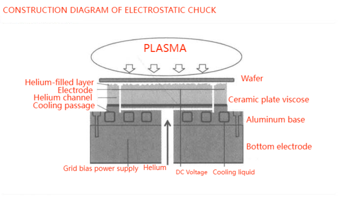
From the material point of view, the electrostatic chuck is mainly based on alumina ceramics or aluminum nitride ceramics as the main material, ceramic materials have good thermal conductivity, wear resistance and high hardness, and compared with metal materials in electrical insulation has inherent advantages. Due to the particularity of its function, the electrostatic chuck requires that its manufacturing material is different from conductor materials and insulator materials, but belongs to semiconductor materials (body resistivity of 10^-3 ~10^10 Ω·cm), so the electrostatic chuck is not pure alumina or pure aluminum nitride material manufacturing. Instead, other conductive substances are added to make the overall resistivity to meet the functional requirements.
According to data from QYResearch, the market sales volume of global electrostatic chuck in 2021 was $1.714 billion, and it is expected to reach $2.412 billion in 2028, with a compound growth rate of 5.06% from 2022 to 2028. From the sales volume point of view, the global sales volume of electrostatic chuck in 2021 is 55,400 pieces, and it is expected to reach 79,900 pieces in 2028. In 2021, the market size of China's electrostatic chuck reached 2.112 billion yuan, and Global InfoResearch forecasted to reach 3.481 billion yuan in 2028, with a compound growth rate of 7.29% from 2022 to 2028.
The global electrostatic chuck market is mainly monopolized by American and Japanese manufacturers, the main manufacturers include the United States Applied Materials, the United States Lam Research, Japan SHINKO, Japan TOTO, Japan NTK companies. Among them, Applied Materials and Lam research company produce electrostatic chuck for their own semiconductor equipment, and they sell the produced etching, PVD, CVD equipment and matched electrostatic chuck to fabs. As electrostatic chuck are consumables, their service life is generally not more than two years, so electrostatic chuck have a large replacement market. In 2021, the world's top three electrostatic chuck manufacturers are Applied Materials, Lam Research and SHINKO, of which Applied Materials ranks first in the world with a market share of 43.86%. Lam Research and SHINKO's market share were 31.42% and 10.20%, respectively.
Fountyl Technologies PTE Ltd, is focusing on semiconductor manufacturing industry, main products include: Pin chuck, porous ceramic chuck, ceramic end effector, ceramic square beam, ceramic spindle, welcome to contact and negotiation!