


News


Nine technological innovations for the semiconductor industry in 2023
From new thermal transistors to faster semiconductor materials, these most important technological innovations are driving the semiconductor industry forward.
1,Introduction of thermal transistor
A revolutionary thermal transistor developed by a team of researchers at the University of California, Los Angeles, has achieved a technological breakthrough. It has unparalleled potential in atomic-level design and molecular engineering for thermal management of computer chips. This new all-solid-state thermal transistor precisely controls the thermal motion inside the semiconducting element through electric field effects. In terms of atomic level design and molecular engineering, thermal management of computer chips has unparalleled potential. And compatibility with current semiconductor manufacturing processes. The transistor achieved a record-breaking switching speed of more than 1 megahertz and provided 1300% tunability in terms of thermal conductivity, exceeding previous limits in terms of thermal conductivity regulation.
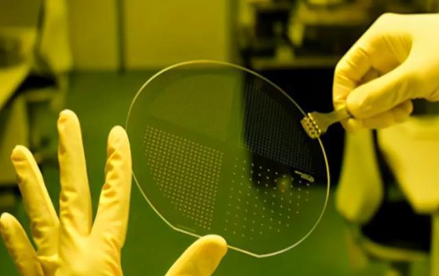
2,EUV Lithography machine upgrade of ASML
In 2023, ASML has delivered its first High-NA EUV scanning lithography machine, Twinscan EXE:5000, to Intel. Collaborative development of the device began in 2018. Intel plans to deploy commercial-grade Twinscan EXE:5200 devices for high-volume production in 2025. The 0.55NA lens of the High-NA EUV scanning lithography machine guarantees a resolution of 8nm, which is essential for advanced chip production above 3nm. By being the first company to adopt this cutting-edge device, Intel has gained a strategic advantage in setting industry standards, potentially surpassing rivals Samsung and TSMC in the future.
3,Artificial intelligence for chip design
Google has shocked the industry with a controversial research paper asserting the power of artificial intelligence in chip design. Google claims that AI technology speeds up the layout planning of the underlying processing units of its AI chips in less than six hours, far exceeding that of human experts. The chip, called the TPU v5, is now causing controversy. Google claims that its aim is not to replace human designers, but to demonstrate that AI can collaborate on chip design.
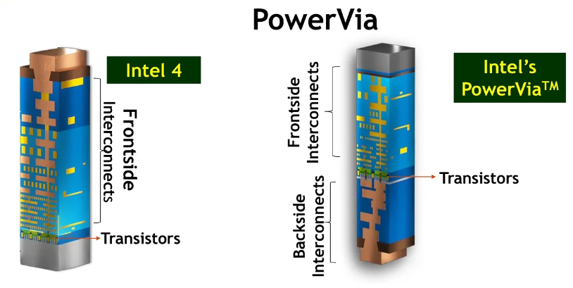
4, Chip reverse power supply technology
Intel is cautiously introducing a new technology, PowerVia, along with RibbonFET. PowerVia uses rear power transmission, placing the power interconnect at the bottom of the silicon material, resulting in a 6 percent increase in frequency, a more compact design, and 30 percent lower power consumption. PowerVia's successful integration into Intel's production process paves the way for 20A nodes with strip FET transistors in 2024, potentially outpacing competitors such as TSMC and Samsung in nanosheet transistors and backside power transmission.
5. Laser integrated chip
Photonic integrated circuits (PICs) have been widely used, deployed in applications such as high-speed optical transceivers and liDAR. However, due to the limited luminous efficiency of silicon, integrating laser onto silicon photonic chips is a big challenge. The nanoelectronics Research and Development Center Imec in Belgium led the research. In flip chip processing, the laser core is precisely aligned to submicron accuracy, transferred and bonded to a silicon photonics wafer.
There are many ways to transfer the laser core, one is the micro pad printing technology, the use of adhesives or molecular bonding, rapid assembly and coupling. It has high application value in high-throughput scenarios where a large number of level 3-5 components need to be integrated. Wafer bonding is another way of 3-5 silicon wafer bonding, which can process multiple devices in parallel and has higher efficiency for optical interfaces.
6,Photon Fusion
Researchers at Stanford University's Congreve Lab are pioneering photochromism with a focus on upfrequency conversion, the process of converting two low-energy photons into one high-energy Photon (Photon Fusion). Using the triplet-triplet annihilation method, which takes advantage of the photosensitive properties of the triplet containing heavy metals, such as palladium, iridium, or platinum, as well as activator materials, such as rubrene, the team has achieved efficient emission of high-energy photons. This process converts wavelengths of light into wavelengths that can be absorbed by silicon solar cells, that is, converting the color of light (color-changing technology). The process has been applied to improve solar efficiency and can increase solar efficiency by 15-20%.
7,Chip-level electron accelerator
Physicists at the University of Erlangen and Nuremberg have made significant advances in chain-sized electron accelerators. Using dielectric materials to make accelerators on the chip, the team created a channel 225 nanometers wide and 0.5 millimeters long that could significantly increase electron energy by 43 percent through precisely timed infrared laser pulses and 733 silicon columns 2 microns high. This provides a major leap forward in the field of accelerator physics, nanophotonic electron accelerators, which can be built using standard clean room techniques such as electron beam lithography.
8,Materials for new high-speed semiconductors
Scientists have discovered what they claim to be the fastest and most efficient semiconductor material to date, Re6Se8Cl2. The material is composed of rhenium, selenium and chlorine, forming clusters known as "superatoms". These superatoms create a unique structure in which excitons, the bound states of electrons and electron holes, bind to phonons instead of scattering states, resulting in new quasiparticles called acoustic exciton-polarons.
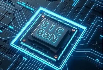
9,Semiconductor sustainability issues: Gallium nitride and silicon carbide
Due to the advantages of gallium nitride (GaN) and silicon carbide (SiC) semiconductors over traditional silicon technology, the field of power electronics is undergoing a sea change. Gallium nitride, based on the field of compound semiconductors, triggered a revolutionary change in the field of lighting around 2001, quickly leading more than 50% of the global gallium nitride LED lighting market. This shift not only reduces lighting electricity consumption by 30 to 40 percent, but also sets the stage for a broader revolution in power electronics. GaN and SiC, which contribute greatly with their superior efficiency and functionality, are replacing silicon in critical power electronics applications. These two materials reduce energy waste and also bring huge environmental benefits.

These new technological advances, while shaping the semiconductor industry, also highlight the development direction of the semiconductor industry in the next few years. The boundaries of technology are constantly being broken, and the only constant is constant innovation.
Fountyl Technologies PTE Ltd, is focusing on semiconductor manufacturing industry, main products include: Pin chuck, porous ceramic chuck, ceramic end effector, ceramic square beam, ceramic spindle, welcome to contact and negotiation!