


News


Semiconductor process equipment: wafer fabrication
The preparation process of wafer: turning sand into silicon wafers on which lines can be carved requires a complex and lengthy process. This news focuses on the following processes: silicon purification, crystal pulling, cutting, polishing, to the production of usable silicon wafers, and some details of the main process. The main contents are process introduction, process objectives, and equipment construction.
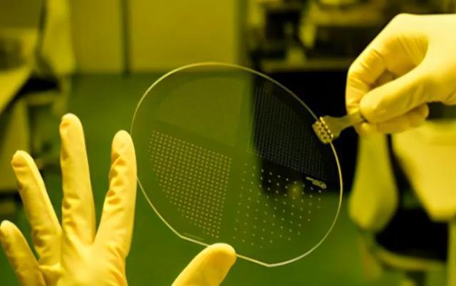
First look at some basic wafer information, and the process route.
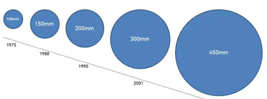
The main wafer sizes are 4 "and 6" silicon wafers, and the current application of 8 "and 12" silicon wafers is expanding. These diameters are 100mm, 150mm, 200mm, 300mm. The increase in the diameter of the silicon wafer reduces the manufacturing cost of a single chip.
Wafer preparation equipment refers to the pure polysilicon material into a certain diameter and length of silicon single crystal rod material, and then the silicon single crystal rod material through a series of mechanical processing, chemical treatment and other processes, into a silicon wafer or epitaxial silicon wafer that meets certain geometric accuracy requirements and surface quality requirements, to provide the required silicon substrate for chip manufacturing equipment.
The typical process for the preparation of silicon wafers with a diameter of less than 200mm is as follows:
Single crystal growth → truncation → outer diameter rolling → slicing → chamfering → grinding → etching → impurity absorption → polishing → cleaning → epitaxy → packaging;
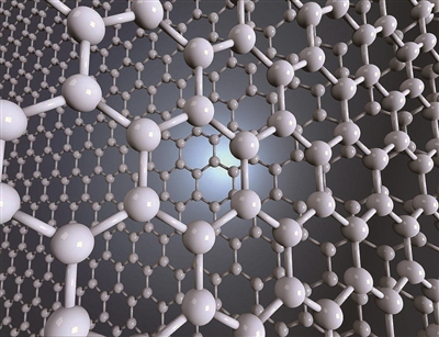
1, Characteristics of silicon materials
Silicon is a semiconductor material because it has four valence electrons and is located along with other elements in the IVA group of the periodic table. The number of valence electrons in silicon puts it right in the middle of a good conductor (1 valence electron) and an insulator (8 valence electrons).
2, Purification of silicon
Pure silicon cannot be found in nature, and it must be refined and purified to become pure silicon needed for manufacturing. It is usually found in silica (silicon oxide or SiO2) and other silicates. Silicon must be purified before it can be used to make chips.
3, Crystal pulling
The process of making monocrystalline silicon from polycrystalline silicon is mainly divided into CZ and FZ. At present, most semiconductor wafers are produced by the czochralase method. Czochralski (Czochralski) method for metal single crystals was invented by Cekolowski in 1916. The monocrystalline silicon clock-pull method includes melting, welding, neck drawing, shoulder placing, shoulder turning, equal diameter growth and finishing steps.
4, Silicon wafer annealling
Effect of annealing furnace: It refers to the process equipment that in the hydrogen or argon environment, the temperature in the furnace rises to 1000 ~ 1200 ° C, and the oxygen near the surface of the polished silicon wafer is volatile from the surface through heat preservation and cooling, so that the oxygen precipitation is layered, the micro-defects on the surface of the silicon wafer are dissolved, the amount of impurities near the surface of the silicon wafer is reduced, the defects are reduced, and the relatively clean area is formed on the surface of the silicon wafer.
Because of the high temperature of the furnace tube of the annealing furnace, it is also called high temperature furnace. The silicon wafer annealing process is also called impurity absorption in the industry.
Silicon wafer annealing furnace is divided into:
· - horizontal annealing furnace;
· - vertical annealing furnace;
· - Rapid annealing furnace.
5, Silicon ingot slice
The headers and trailers of ingot are cut off and the dimensions are tested (to determine the process parameters for subsequent processing). At present, the more commonly used method is multi-wire cutting, which has higher efficiency and better cutting quality
Multi-wire cutting is a new cutting method in which the abrasive is brought into the semiconductor processing area for grinding through the high-speed reciprocating movement of the metal wire, and the hard and brittle materials such as semiconductors are cut into hundreds of sheets at the same time. CNC multi-wire cutting machine has gradually replaced the traditional inner circle cutting, becoming the main way of silicon wafer cutting processing.
6, Round edges and grinding surface
When an ingot is cut into a wafer, it will form a sharp edge, with edges, burrs, chipping, small cracks or other defects. The edge shape and outer diameter of the wafer need to be adjusted to avoid the influence of edge cracking on the wafer strength, damage to the surface of the wafer and bring pollution particles to the post-process. The grinding process removes the saw marks and breakage on the wafer surface during cutting, so that the wafer surface meets the required finish.
7, Etching
A chemical solution is used to etch away the damaged layer on the wafer surface caused by processing pressure.
8, Polishing
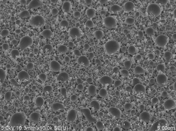
Wafer polishing using ultra-fine slurry (particle diameter 10~100 nm, composed of Al2O3, SiO2 or CeO2), combined with pressure, erosion, mechanical and chemical methods to polish the wafer surface between the two rotating gaskets, to obtain excellent surface flatness.
The polishing process (hereinafter referred to as polishing method) can be divided into the following three categories in principle according to the action between the polishing liquid and the surface of the silicon wafer.
1. Mechanical polishing
At present, the mechanical polishing method is generally no longer used in industry.
2. Chemical polishing
In industrial production, chemical polishing is usually only used as a pre-treatment before polishing, rather than as a polishing process alone.
3. Chemical mechanical polishing method(CMP)
Chemical mechanical polishing method uses the dual effect of polishing liquid on the surface of silicon wafer mechanical grinding and chemical corrosion, and has the advantages of both mechanical polishing and chemical polishing. CMP is one of the technologies developed by the industry to manufacture large-diameter wafers, and it is the most commonly used polishing method in the modern semiconductor manufacturing industry.
9, Cleaning
Clean wafers thoroughly with ultra-pure chemicals to remove contaminants from the process
10, Inspection
Through optical inspection, ensure that the wafer size, shape, surface finish, flatness and other technical indicators meet the specifications.
Fountyl Technologies PTE Ltd, is focusing on semiconductor manufacturing industry, main products include: Pin chuck, porous ceramic chuck, ceramic end effector, ceramic square beam, ceramic spindle, welcome to contact and negotiation!