


News


Semiconductor technology and equipment: lithography technology and equipment
Part One: the process of lithography
Photolithography is a pattern transfer technique in which the pattern on the mask plate is transferred to a silicon wafer coated with a photoresist (or photoresist), and a specific part of the film on the surface of the silicon wafer is removed through a series of production steps.
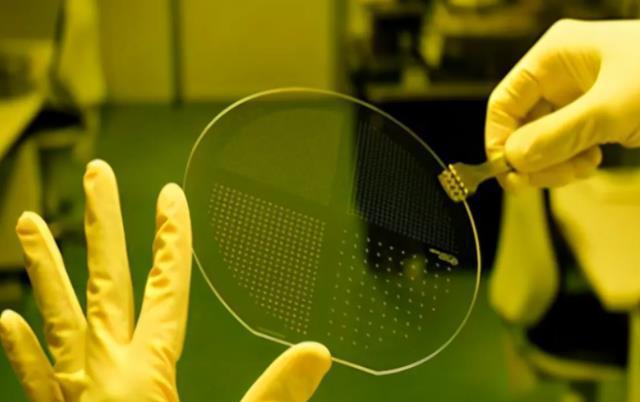
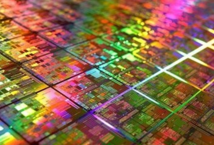
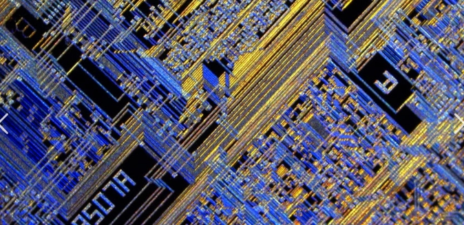
Lithography technology is a key semiconductor technology developed on the basis of photographic technology and flat printing technology. It is easy to understand that integrated circuit manufacturing is to manufacture hundreds of millions of devices in batches on the area of a few square centimeters, and the structure of each device is also quite complex, as shown in the following figure, is a seemingly difficult to clear the internal structure of the chip.
This manufacturing density is equivalent to making tens of millions of such transistors in the cross-sectional area of a human hair.
The second part: lithography equipment
Lithography machines have been around since the 1960s. Early lithography techniques were not particularly difficult things, after all, the line width required for lithography at that time was in the micron level. So the lithography machine is also very simple, even when Intel directly removed the 16 mm camera lens can be used. Only a handful of companies, such as GCA, K&S and Kasper, produced a handful of such devices, and lithography machines were not high-tech at all, not much more complicated than cameras.
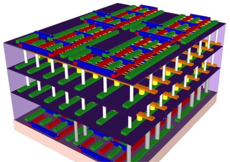
However, as the number of transistors continues to double, the exposure accuracy quickly from a few microns to a few tenths of a micron, so these simple lithography machines are difficult to meet the demand, and more and more problems. After the transistor is more, the interconnection has increased a lot, the need for multi-layer metal connection, the metal layer needs to be stacked on the medium layer, the need for different exposure graphics on the medium layer wiring, the need for different light cover repeated exposure, so the repeated alignment accuracy has become a big problem, just like building, each layer must be aligned up and down, can not cover the cover oblique. In the integrated circuit process, this accuracy is required to be extremely accurate, reaching the nanometer level...
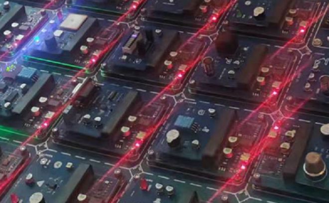
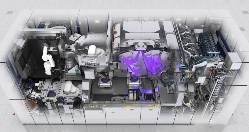
At this time, the lithography machine has been from the early extremely simple equipment, into the current collection of precision optics, laser, fluid physics, electromagnetic, precision control, machining, electronic information, electronic circuits, chemistry and other dozens of disciplines of cutting-edge technology in one, is currently the most sophisticated and expensive industrial equipment. ASML's high-end lithography machines sell for more than $100 million, comparable to an airplane. The early lithography machine is called Mask Aligner, which means the mask aligner exposure, and now the word lithography is used to refer to the lithography machine and the lithography process.
The following are some of the main types of lithography machines, and some brief descriptions of the main characteristics of each type. The sequence is arranged in the way of the gradual improvement of the technology, and it is helpful to understand the lithography technology from simple to deep.
- Mask Aligner
- Contact Photolithography
- Stepper Photolithography
- Sacnner Photolithography
- Immersion
- DUV/EUV
Below we introduce the details of each lithography machine
Mask Aliger
It is the most direct lithography application. The simplest mask alignment exposure can be the "manual" device in the image below, where mask alignment is achieved through a microscope and manual adjustment, and photolithography is performed through exposure.
Contact Photolithography
Contact lithography is lithography using a mask calibrator. The mask aligner has two main tool structures: the mask holder and the wafer holder. The mask holder is machined to a very flat surface on which the photomask is fixed by vacuum. The wafer holder, which is also machined very flat, is also vacuumed to keep the wafer in place. This tool ensures that the surfaces of the two parts remain parallel to each other during operation. The wafer holder can be moved up onto the mask holder in order to use variable forces to bring the wafer into contact with the mask. The surface position of the chip chuck can also be adjusted to be as flat as possible with the mask for best results; This is called wedge error compensation. Once the wafer and mask are in place, exposure can be performed by opening the shutter on the lampshade. Inside the lampshade is a mercury arc lamp and associated optics, which will allow a selected controlled UV band to expose the mask and wafer.
stepper Lithography
Stepper lithography is for smaller and finer chips, by adjusting the position of the wafer in a progressive way, multiple exposures on a single wafer. Also known as Step and repleat System.
sacnner Photolithography
There are two broad categories of projection lithography tools - scanning and step and repeat systems.
Scanning projection printing is pioneered by Perkin-Elmer [1.5], uses reflective optics (i.e. mirrors rather than lenses) to project light from the slit in the mask onto the wafer when both the mask and wafer are moved by the slit at the same time. The irradiation dose is determined by the intensity of the light, the width of the slit, and the speed at which the wafer is scanned. These early scanning systems used multicolor light from a mercury arc lamp that was 1:1, meaning the mask and the image were equal in size.
Stepper and repeat cameras (stepper cameras for short) expose a rectangular portion of the wafer (called the image field) at one time, either 1:1 or reduced in size. These systems use refraction optics (i.e., lenses) and are usually quasi-monochromatic. Both types of systems (Figures 1-5) are capable of high resolution imaging, although the highest resolution requires restoration imaging.
By the mid-1970s, scanners replaced near-printing for devices smaller than 4 to 5 μm in size. By the early 1980s, as device designs were pushed below 2 μm, steppers began to dominate. With minimum feature sizes reaching the 250 nm level, steppers continued to dominate lithography throughout the 1990s. By the early 1990s, however, Perkin-Elmer's successor, SVG Lithography, introduced a hybrid step scanning method.
The step scanning method uses a small portion of the normal step approach (e.g., 25mm x 8mm) and then scans that field in one direction to expose the entire 4 x reduction mask. Then move the wafer to a new location and repeat the scan. Smaller imaging fields simplify lens design and manufacturing, but at the cost of more complex apertures and wafer pads. Step-scanning technology is the technology of first choice for manufacturing below 250nm today.
Immersion Lithography
Immersion lithography is a lithographic enhancement technique that replaces the usual air gap between the final lens element and the photoresist surface with a liquid medium with a refractive index greater than 1. Smaller wavelengths in liquids allow imaging of smaller features, currently using water as a liquid. Immersion technology was first introduced by Carl Zeiss in the 1880s to improve the resolution of optical microscopes. In the 1980s, immersion technology was introduced into modern lithography. Since 2002, Immersion has grown incredibly fast.
DUV/EUV
Lithography systems have evolved from blue wavelengths (436nm) to ultraviolet (UV:UtraViolet, 365nm) to Deep ultraviolet (DUV:Deep UltrViolet, 248nm) to today's mainstream high-resolution wavelength of 193nm. With the development of projection tools and various other technologies, DUV technology can be used to produce features smaller than 100 nanometers in size. In recent years, with the use of overlap offset technology, DUV technology has also continued to advance, and the production capacity has been continuously reduced to 50 nm, 28 nm, and even 7 nm. Extreme ultraviolet lithography is an X-ray technique with a wavelength of 13.5nm. Today's EUV scanners can achieve resolutions as low as 22nm half-pitch. In the system, the EUV light source uses a high-power laser to generate plasma. This, in turn, helps to emit short-wavelength light in the vacuum chamber.
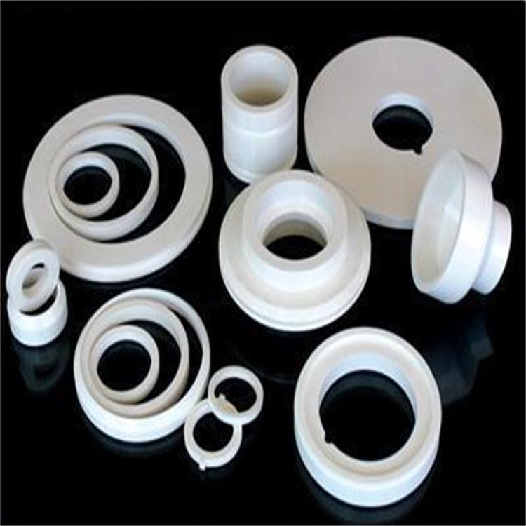
Fountyl Technologies PTE Ltd, is focusing on semiconductor manufacturing industry, main products include: Pin chuck, porous ceramic chuck, ceramic end effector, ceramic square beam, ceramic spindle, welcome to contact and negotiation!