


News

Summary of common semiconductor manufacturing processes
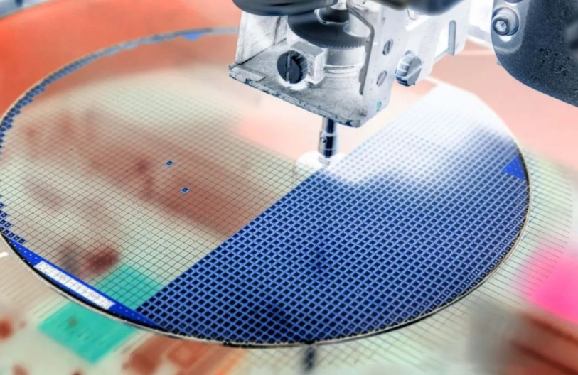
Semiconductor manufacturing refers to the process of machining a complete chip that can achieve a specific function on a wafer through a series of complex steps. Different chip products involve different processes, so we will systematically introduce all semiconductor processes that may be involved in semiconductor manufacturing.
What are the boundaries between semiconductor manufacturing and packaging?
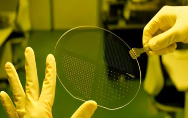
Unlike the purpose of packaging, semiconductor manufacturing (Front-end) aims to produce bare wafers with complex circuit patterns and needs to be carried out in a highly controlled clean room environment to prevent dust from affecting the tiny circuit structure. The goal of packaging (Back-End of Line) is to protect the bare chip and enhance the physical strength and environmental tolerance of the chip. Generally, wafer thinning is used as the dividing point between manufacturing and packaging, and the wafers after thinning are shipped from the wafer fab to the packaging factory, so the semiconductor manufacturing process ends.
What are the process differences between different chip products?
Chip is a very broad concept, is a large category, so it is subdivided into many categories. Generally, it can be divided into logic chips (CPU, GPU, etc.), memory chips (DRAM, NAND, Flash, etc.), analog and mixed-signal chips, power devices, RF chips, sensor chips, etc.
Different types of chip products use different design principles, process standards and material choices according to their application and functional requirements. For example, we often say that the 5nm, 7nm advanced chip process is usually used in logic chips, and for the RF chip field SAW, BAW, etc., does not take line width as a consideration. For example, the memory chip is mainly 12 inches, but the third-generation semiconductor is generally used 4,6 inches due to the limitation of the SiC substrate.
Semiconductor Manufacturing Process Classification?
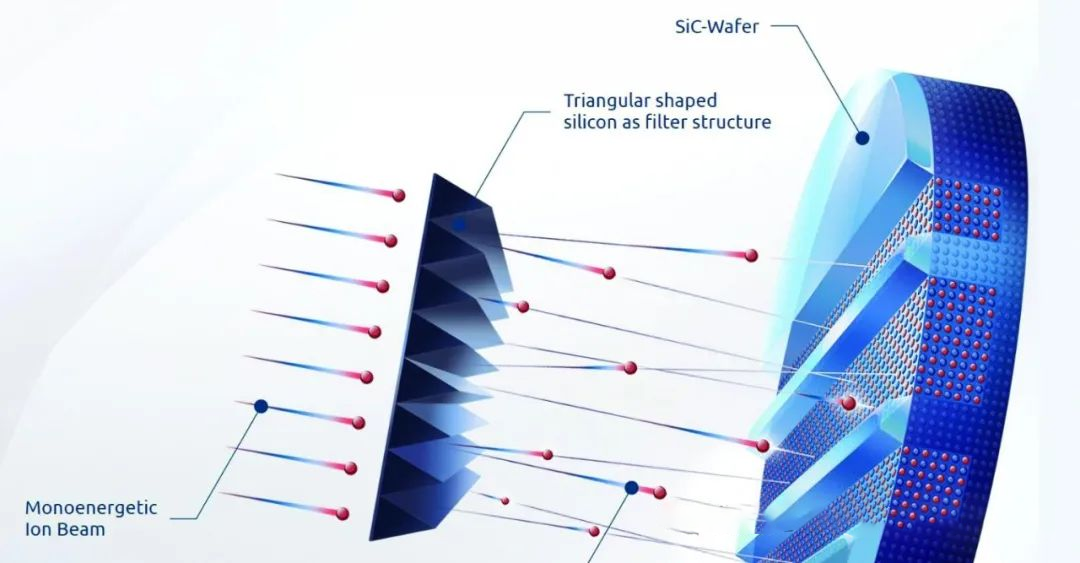
Photolithography includes coating, exposure, development, baking and other processes. Dry coating: including PVD(physical vapor deposition), CVD (chemical vapor deposition), ALD (atomic layer deposition). PVD also includes Evaporation (Evaporation), Sputtering (Sputtering), pulsed Laser deposition (PLD), etc. CVD includes plasma enhanced CVD (PECVD), low pressure CVD (LPCVD), metal-organic CVD (MOCVD),MPCVD, Laser CVD. Dry etching such as APCVD, HT-CVD, UHV CVD: Dry etching is divided into physical etching, chemical etching, physical chemical etching. Physical etching includes ion beam etching (IBE), chemical etching includes plasma deadhesive machine, etc. Physical and chemical etching includes ICP-RIE,CCP-RIE,ECR-RIE,DRIE, etc. Epitaxy: It is divided into liquid phase epitaxy (LPE), gas phase epitaxy (VPE), molecular beam epitaxy (MBE), chemical beam epitaxy (CBE), etc. Ion Implantation: including High energy ion implantation, low energy ion implantation, high dose ion implantation, high flux ion implantation, High Mass Molecular Ion Implantation, etc.
Diffusion: gas source diffusion, liquid source diffusion, solid source diffusion, pre-deposition diffusion, etc
Annealing: furnace tube annealing, rapid thermal annealing, laser annealing, plasma annealing and other wet methods Wet methods are divided into wet etching, cleaning, electroplating, electroless plating, cmp and so on.
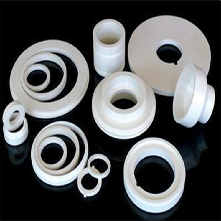
Fountyl Technologies PTE Ltd, is focusing on semiconductor manufacturing industry, main products include: Pin chuck, porous ceramic chuck, ceramic end effector, ceramic square beam, ceramic spindle, welcome to contact and negotiation!