


News

What is the difference between substrate and epitaxy?
In the semiconductor industry chain, especially in the third generation semiconductor (wide band gap semiconductor) industry chain, there will be a substrate and epitaxial layer, what is the significance of the existence of epitaxial layer? What's the difference from the substrate?
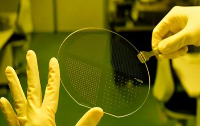
In the process of wafer preparation, there are two core links: one is the preparation of substrate, and the other is the implementation of epitaxial technology. The substrate, a wafer crafted from a semiconductor monocrystalline material, can be used as the basis for direct input into the wafer fabrication process to produce semiconductor devices, or further enhance performance through an epitaxial process.
So, what is epitaxy? In short, epitaxy is the growth of a new layer of single crystals on top of a single crystal substrate that has been finely treated (cut, ground, polished, etc.). The new single crystal and substrate can be of the same material or different materials, so that homogeneous or heterogeneous epitaxy can be achieved as needed. Because the newly grown single crystal layer will expand according to the crystal phase of the substrate, it is called the epitaxial layer. Its thickness is generally only a few microns, taking silicon as an example, silicon epitaxy growth is on a silicon single crystal substrate with a specific crystal direction, and then grow a layer of silicon single crystal layer with the same crystal direction as the substrate, the resistivity and thickness is controllable, and the lattice structure is perfect. When the epitaxial layer grows on the substrate, the whole is called an epitaxial sheet.
For the traditional silicon semiconductor industry, the production of high-frequency high-power devices directly on silicon wafers will encounter some technical difficulties, such as the requirements of high breakdown voltage, small series resistance and small saturation voltage drop in the collector area. The introduction of epitaxy technology solves these problems skillfully. The solution is to grow an epitaxial layer with high resistivity on a silicon substrate with low resistivity, and then fabricate devices on the epitaxial layer with high resistivity. In this way, the high-resistivity epitaxial layer provides a high breakdown voltage for the device, while the low-resistivity substrate reduces the resistance of the substrate, thereby reducing the saturation voltage drop, thus achieving a balance between high breakdown voltage and small resistance and small voltage drop.
In addition, GaAs and other Ⅲ-Ⅴ group, Ⅱ-Ⅵ group and other molecular compound semiconductor materials of vapor phase epitaxy, liquid phase epitaxy and other epitaxy technology have also been greatly developed, has become the vast majority of microwave devices, optoelectronic devices, power devices and other indispensable process technology. In particular, the successful application of molecular beam and metal-organic gas phase epitaxy technology in thin layer, superlattice, quantum well, strain superlattice and atomic-level thin layer epitaxy has laid a solid foundation for the development of a new field of semiconductor research "energy band engineering".
As far as third-generation semiconductor devices are concerned, these semiconductor devices are almost all done on the epitaxial layer, and the silicon carbide wafer itself only acts as the substrate. The thickness of SiC epitaxial material, background carrier concentration and other parameters directly determine the electrical properties of SiC devices. Silicon carbide devices with high voltage applications require new parameters such as thickness of epitaxial material and background carrier concentration. Therefore, silicon carbide epitaxy technology plays a decisive role in the full play of the performance of silicon carbide devices, almost all SiC power devices are based on high-quality SiC epitaxy sheet, epitaxy layer production is an important part of the wide band gap semiconductor industry.
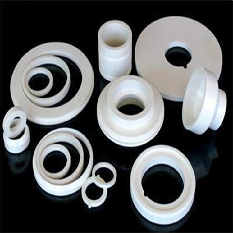
Fountyl Technologies PTE Ltd, is focusing on semiconductor manufacturing industry, main products include: Pin chuck, porous ceramic chuck, ceramic end effector, ceramic square beam, ceramic spindle, welcome to contact and negotiation!