


News
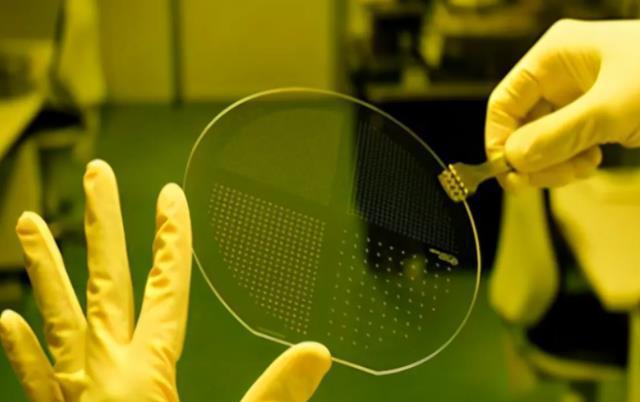
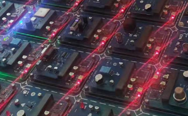


X-ray applications in chip manufacturing
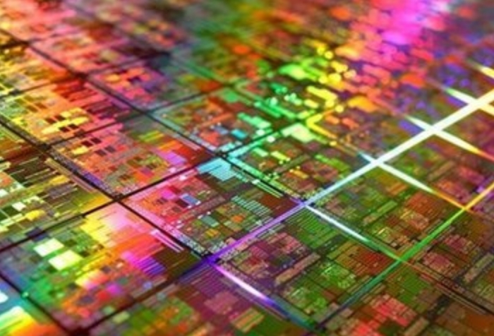
X-rays are widely used in production and life, and the importance of semiconductor manufacturing is self-evident. Today, let's talk about the application of X-rays in semiconductor manufacturing.
What are X-rays?
X-ray is a kind of electromagnetic wave. Electromagnetic waves are ordered according to the size of the wavelength, in order: Radio Waves > Microwaves > Infrared > Visible Light > Ultraviolet > X-ray > Gamma rays. The shorter the wavelength of the electromagnetic wave, the higher the frequency and the stronger the energy.
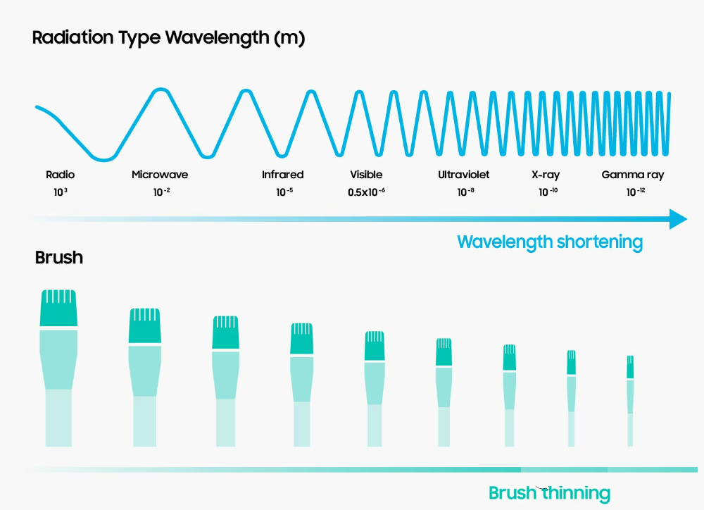
With a wavelength range of 0.01 to 10 nanometers, it has a high energy and is by far the most penetrating electromagnetic wave except for gamma rays. Because the wavelength is so short, X-rays are generally referred to in terms of energy rather than wavelength. X-rays were discovered by the German scientist Wilhelm Conrad Roentgen in 1895, and because their nature was unknown at the time, they were named "X-rays". He found that X-rays from the arms and hands could produce detailed images of the internal bones. That's because the bone is dense and absorbs more X-rays than the skin, so the X-ray film leaves a shadow of the bone while the skin appears transparent. In 1896, he published his findings in the Journal of Physics. His discovery attracted worldwide attention and revolutionized medical imaging. Roentgen won the first Nobel Prize in Physics for this in 1901, so X-rays are also called Roentgen rays. X-ray Diffraction (XRD) in Semiconductor Manufacturing
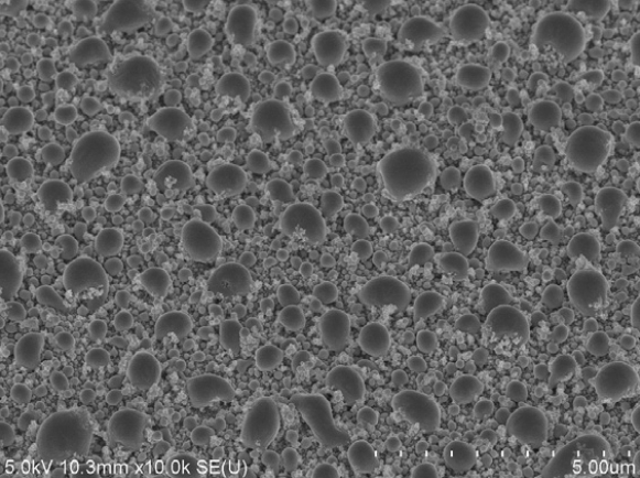
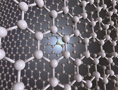
XRD is a technique used to identify the atomic and molecular structures inside crystals. The crystal structure and chemical composition of the sample can be deduced by measuring the diffraction Angle and intensity of the ray from the crystal structure within the sample. The basic principle of X-ray diffraction is Bragg's Law, which describes that the intensity of the rays will be maximum at a particular Angle when they are reflected in the crystal plane. This Angle is dependent on the lattice parameters of the crystal.
X-ray Fluorescence Spectrometry (XRF)
XRF It can be used to determine the elemental composition of a material, with the advantage that it can nondestructively analyze the sample and usually does not require complex pretreatment of the sample. XRF works based on the atomic structure of each element. When a substance is bombarded with X-rays or high-energy electrons, its inner electrons are knocked out of the atom by the rays or electrons, causing the atom to be in an excited state. To restore stability, an outer electron will transition to the inner vacancy, emitting an X-ray photon at the same time. The energy of this photon is equal to the energy difference between the two electron shells, and this energy difference is specific to each element. Therefore, by measuring the energy of the emitted X-rays, we can determine the elements in the sample.
CT is an important non-destructive detection tool. A CT scan can produce a three-dimensional image of the inside of a semiconductor device, helping engineers conduct a comprehensive inspection and analysis of the device. The principle of X-ray production in a device usually uses an "X-ray tube" to produce X-rays. First, electrons are emitted in the cathode by superheating. These electrons are then accelerated to high speeds, and the accelerated electrons collide with the anode (usually made of tungsten or other metal). During the high-speed movement and collision between the cathode and anode, the electrons lose energy. When an electron passes through this process, it converts some or all of its energy into X-rays. The resulting X-rays are emitted through a window.
Fountyl Technologies PTE Ltd, is focusing on semiconductor manufacturing industry, main products include: Pin chuck, porous ceramic chuck, ceramic end effector, ceramic square beam, ceramic spindle, welcome to contact and negotiation!