

Main product
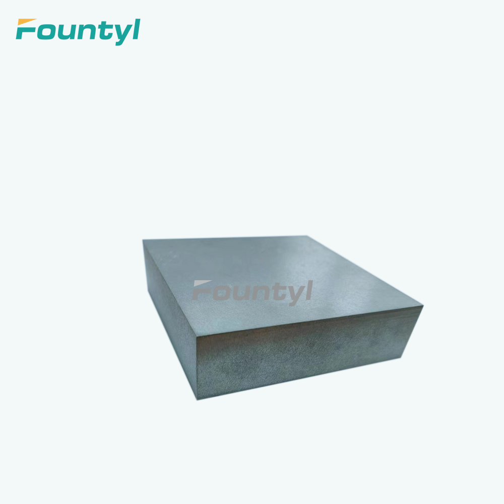
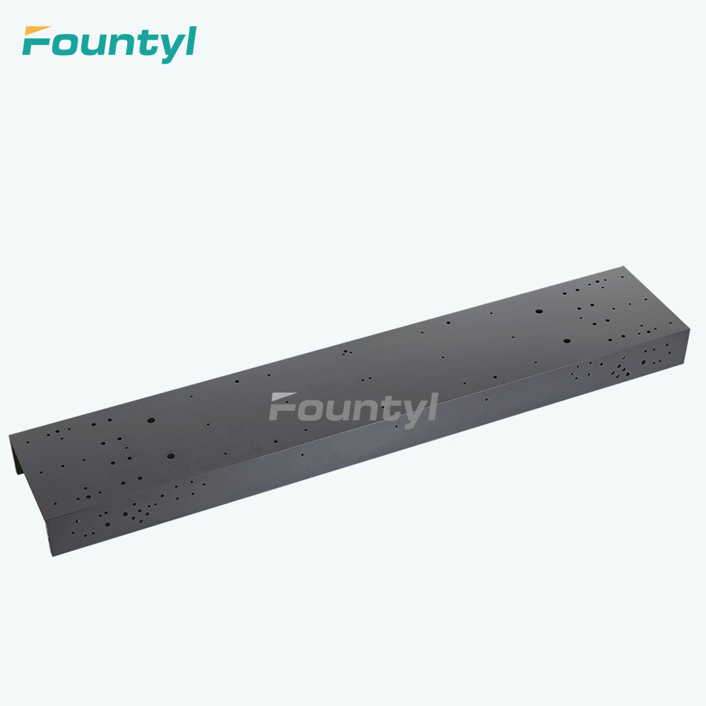
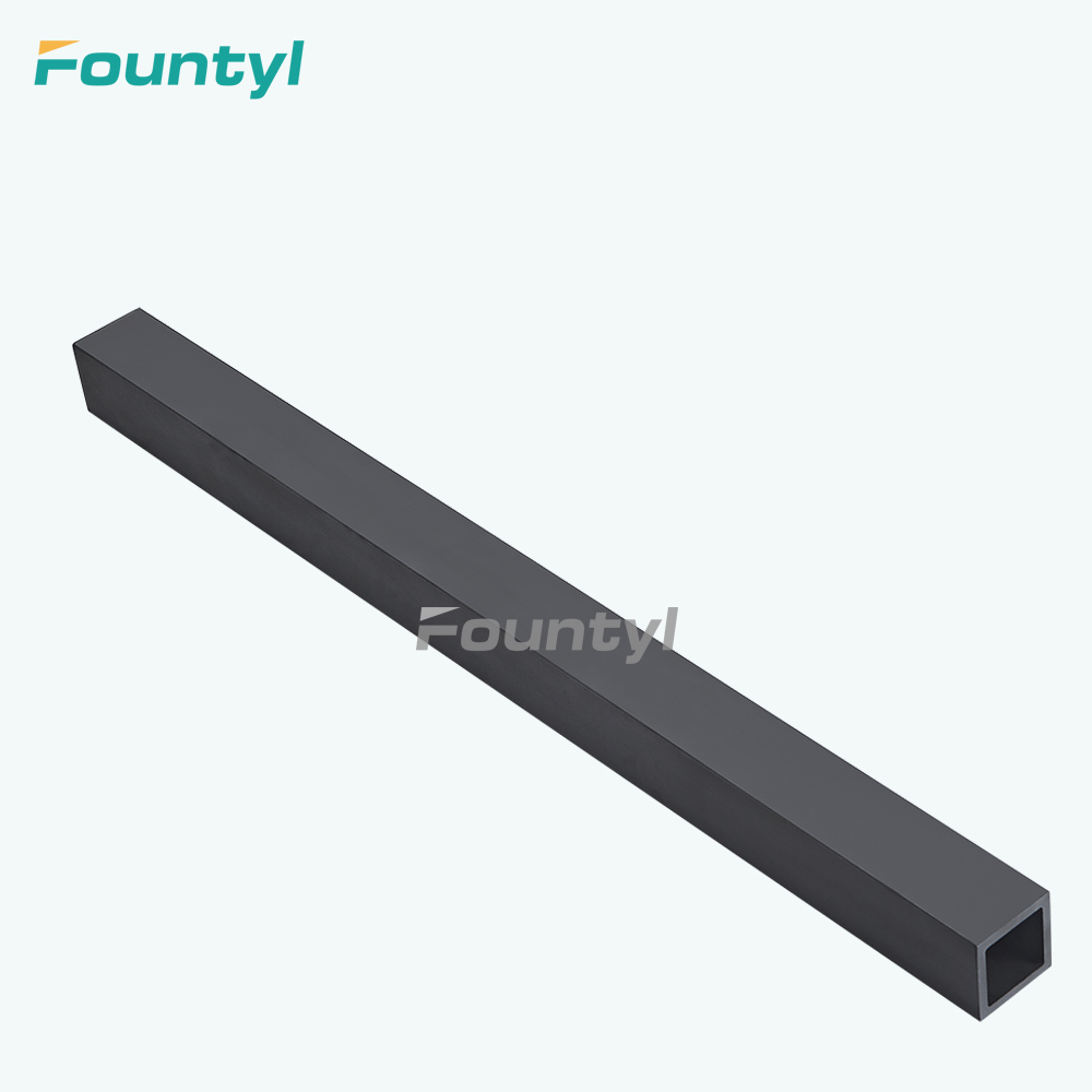
Square beam & guide rail for ultra-precision motion platform and detection equipment
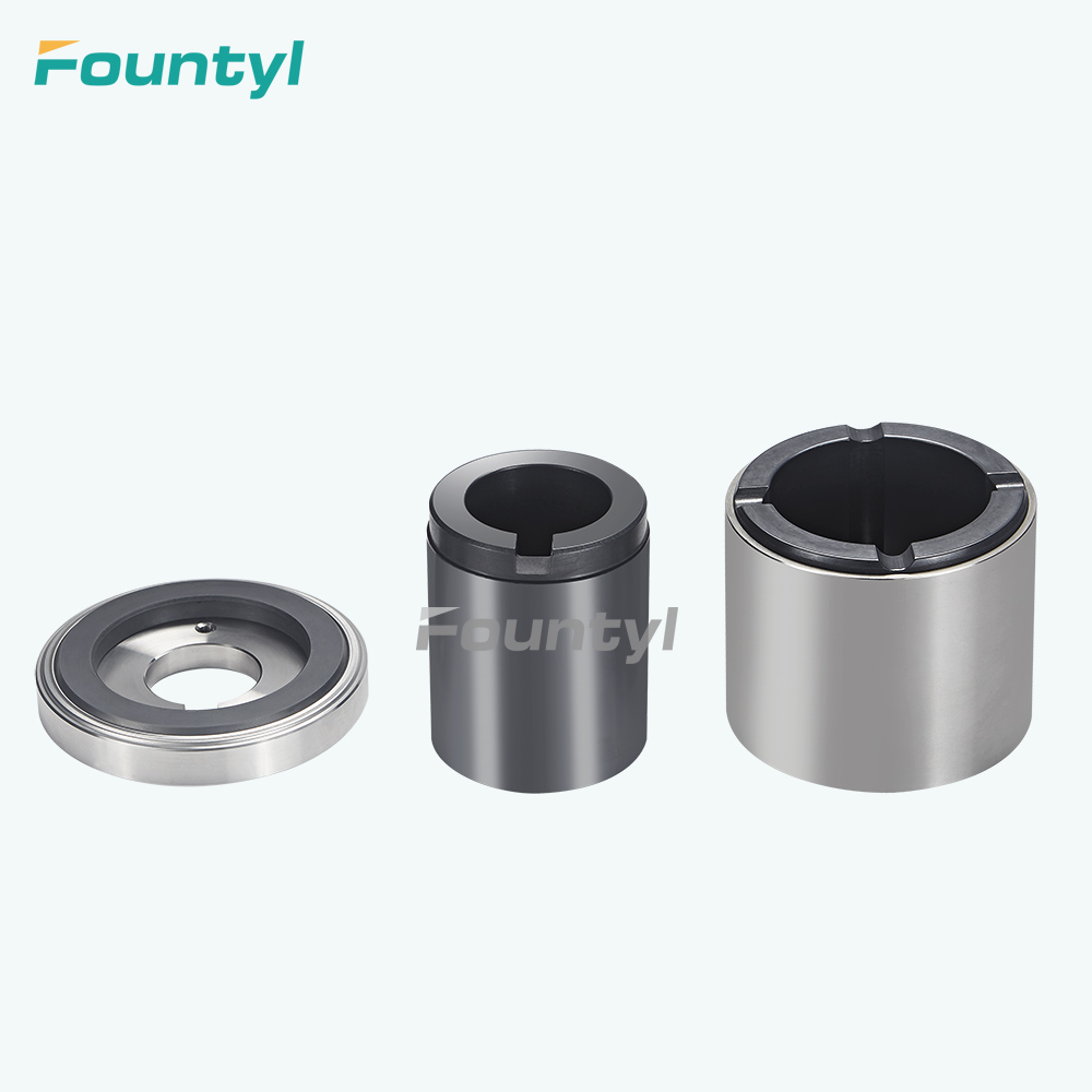
Taking the vacuum chuck assembly as an example, the material used in the earliest 2 inch and 4 inch wafer era is aviation aluminum, but it has encountered the bottleneck of ultra-high flatness (better than 1 micron) in the era of large-size wafers (8 "and more than 8"), which cannot meet the hard index of ultra-high flatness and is eliminated. Next, alumina material as a transition, its elastic modulus, light weight, thermal conductivity and expansion coefficient and silicon carbide dwarf, but not on some embarrassing; After the breakthrough in the preparation technology of large-size and complex special-shaped hollow structure silicon carbide ceramics, components including ultra-precision workpiece base, ultra-precision air float guide, and wafer transmission arm have been upgraded.
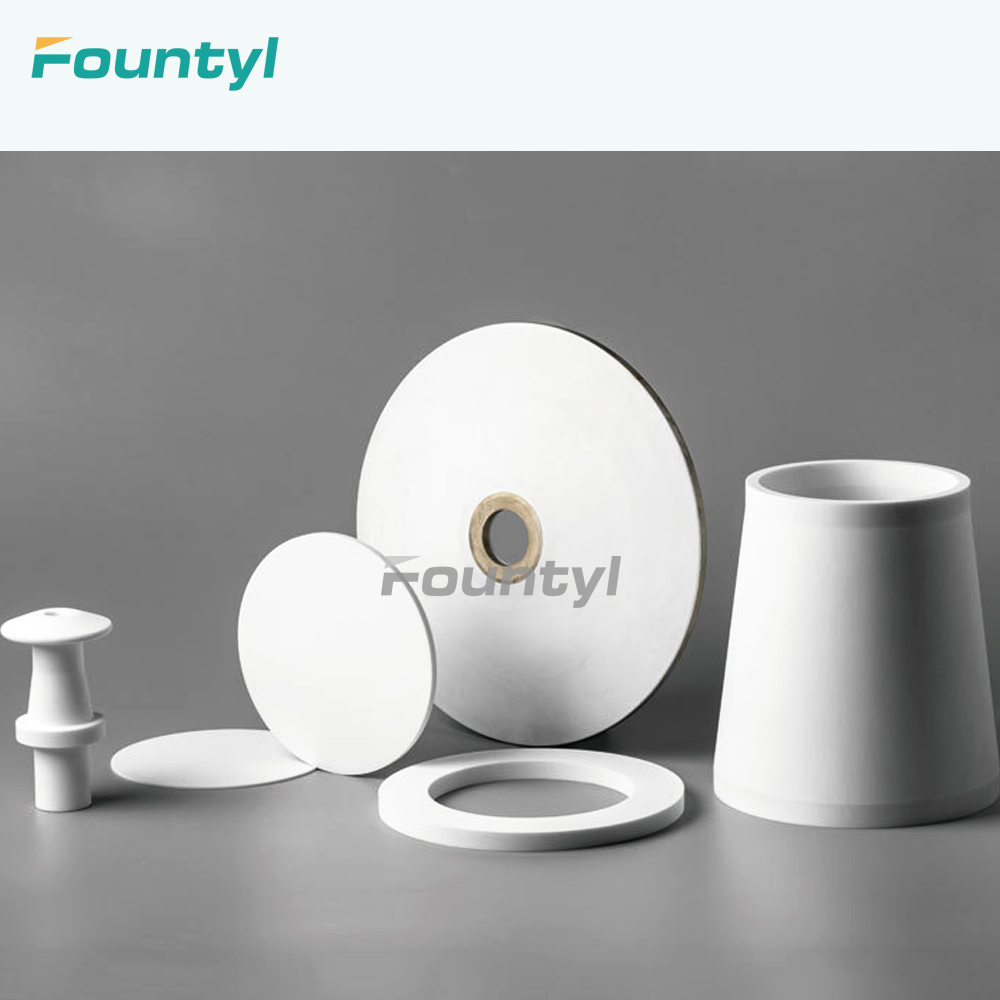
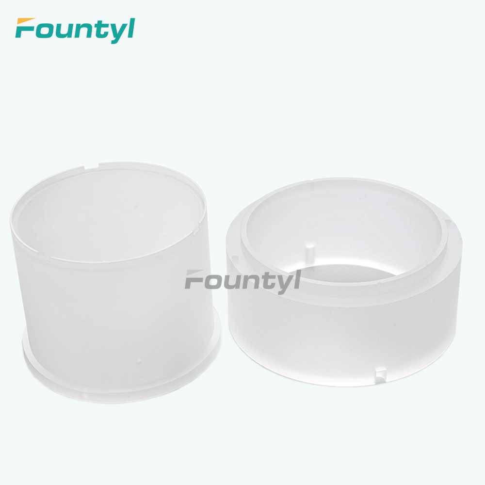
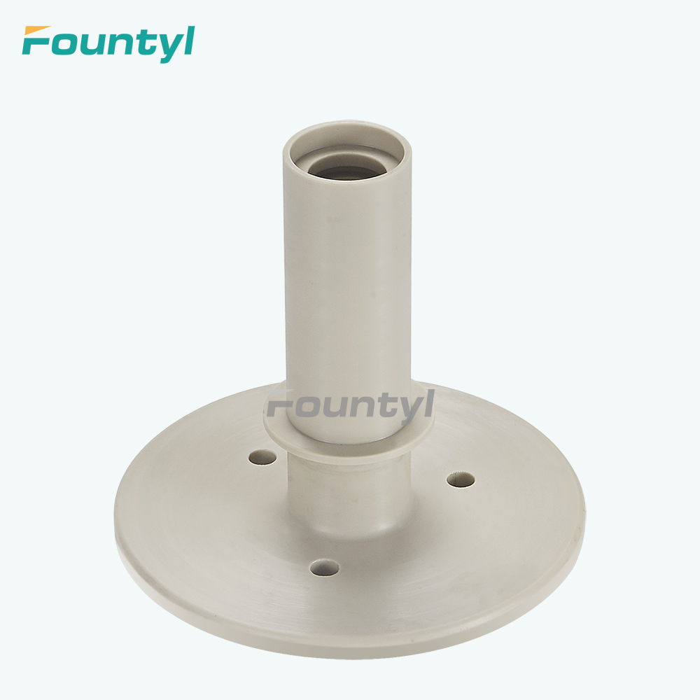
Not only the above-mentioned silicon carbide ceramic parts that meet the ultra-high precision hard indicators on flatness, parallelism, and verticality, for the high-purity silicon carbide ceramic parts required for the wafer diffusion, doping, etching processes in the semiconductor industry, especially in the high-purity CVDSiC material preparation technology, has a mature process technology, and has realized the manufacture of high-purity silicon carbide ceramic crystal boat, silicon carbide ceramic bearing plate, silicon carbide ceramic air floating movement platform, silicon carbide ultra-precision moving platform, silicon carbide guide rail, silicon carbide slide rail components.
In the future, we will further expand the application of silicon carbide materials in the semiconductor industry and contribute to the upgrading of the semiconductor industry chain and silicon carbide ceramic industry. China's precision silicon carbide ceramic components independent research and domestic application promotion has just started, with the vigorous development of semiconductor industry, the market demand for this kind of high-end ceramic structure will be more and more large, silicon carbide with its excellent physical and chemical properties, in the semiconductor industry has broad application prospects.
Silicon carbide ceramics not only have excellent mechanical properties at room temperature, such as high bending strength, excellent oxidation resistance, good corrosion resistance, high wear resistance and low friction coefficient, but also high temperature mechanical properties (strength, creep resistance, etc.) are the best known ceramic materials. Silicon carbide has the characteristics of corrosion resistance, high temperature resistance, high strength, good thermal conductivity, impact resistance...etc.
The requirements of lithography machine for workpiece table structure: Ultra-lightweight (reduce motion inertia, reduce motor load), ultra-high stability (ultra-precision machining requires high-precision motion and positioning, requiring minimal dimensional deformation of thermal expansion and other factors), cleanliness (high hardness and high wear resistance), It can meet the technical requirements of large size, hollow thin wall, complex structure and precision silicon carbide structural parts for the key equipment of integrated circuit manufacturing represented by photolithography machine.
Fountyl Capabilities
Maximum size: 1600mm.
Structure customization: lightweight structure, can be designed to reduce weight structure.
High accuracy: Flatness can be controlled within 5 microns or even higher accuracy.