


News


Chip industry. Technical terms and abbreviations. Graphic analysis of nouns
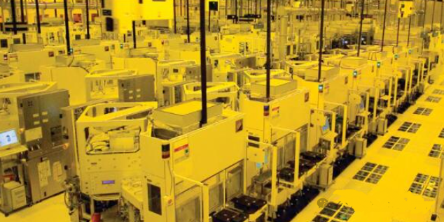
Manufacturing
TAPEOUT(TO): It means to submit the final GDSII file to Foundry for processing.
FULL MASK: That is, all masks in the manufacturing process serve a certain design.
MPW (Multi Project Wafer): That is, multiple projects share a wafer, that is, the same manufacturing process can undertake the manufacturing task of multiple IC designs.
MPW is to share a MASK plate with other manufacturers, and FULL MASK is to enjoy alone a mask plate. If the chip risk is relatively high, you can do MPW first, if the test is no problem, and then do FULL MASK.
Foundry: Specialized in chip manufacturing manufacturers, such as Taiwan Semiconductor Manufacturing (TSMC), Semiconductor Manufacturing International (SMIC), United Electric (UMC). The corresponding is fabless, is the design manufacturer, just no fabs.
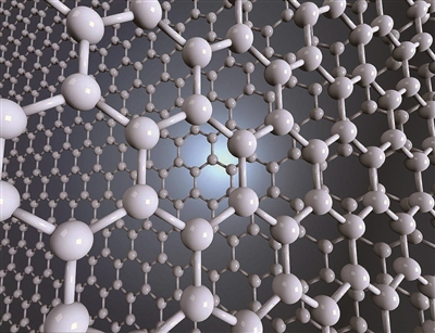
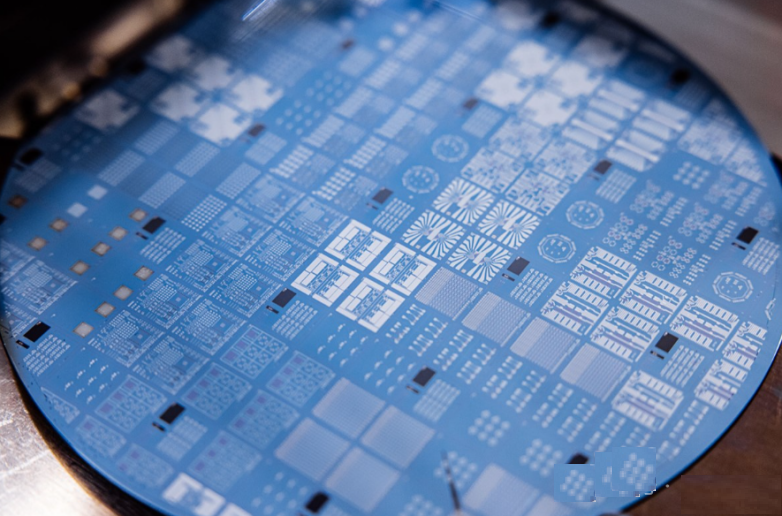
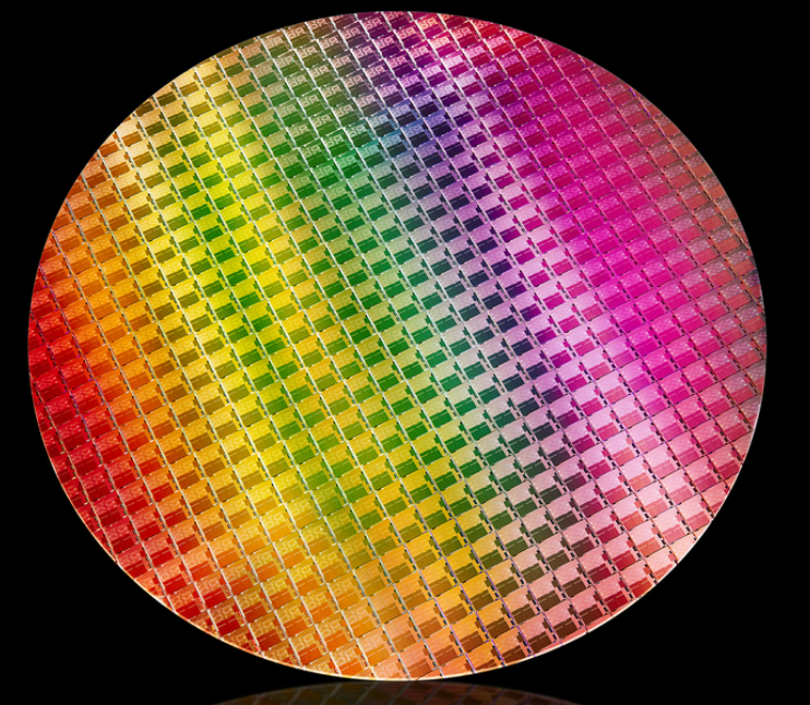
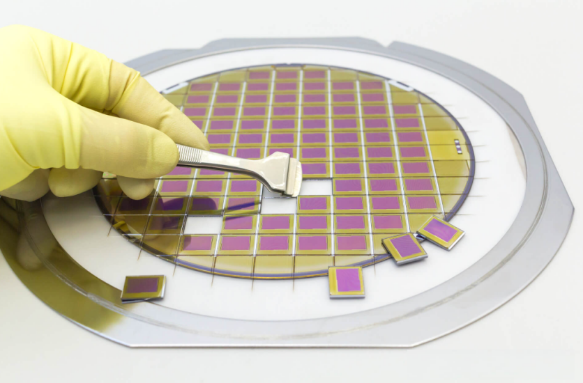
Wafer
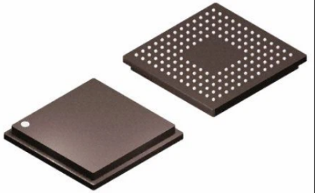
Die:After the wafer is cut, the wafer of a single chip, which needs to add a sealed shell to become a chip.
Chip: The final package of the chip
Bump:bumping refers to bumping points. After a convex point (gold, tin lead, lead-free...etc.) is grown on the surface of the wafer, (mostly used on the flip process package, that is flipchip).
Mask :Mask an opaque graphic template in the selected area on the wafer, and subsequent corrosion or diffusion will only affect the area outside the selected area
Chamber:Refers to a confined space and has a special purpose, such as vacuuming, gas reaction or metal sputtering.
Dicing Wafer:Wafer dicing, wafer cutting

CVD (Chemical Vapor Deposition) :It is an advanced technology that is widely used in the field of material preparation, using high temperature and low pressure environments to convert chemicals in gases or gas mixtures into solid materials.
PVD (Physical Vapor Deposition):A method of attaching another material to the surface of a substrate by ion plasma technology. Is the general name of spray, evaporation...etc.
CMP (Chemical-Mechincal Polish): The use of grinding pad (polishingpad) covered with grinding particles on the surface, , with the aid of chemical additives (reagent), with chemical reaction and mechanical grinding of double processing action, to carry out its surface flatness treatment on the uneven crystal surface.

CDA (Clean Dry Air) : Usually refers to air with a pressure between 60 and 110psi, which has been purified and dried. As a gas source for pneumatic components.
Diffusion: In the semiconductor industry, it is often used as a diffusion source on a very pure silicon chip by presetting or ion implantation, and the diffusion is completed within a few hours by adding high temperature to the furnace tube
DI Water: Tap water or groundwater, containing a large number of bacteria, metal ions and particles, must be sterilized and purified by equipment, and then the impurities of metal ions removed, the Derived water is called "deionized water". Designed for IC manufacturing.
Dopant: In the original semiconductor material, the active implantation or the incorporation of other atoms or ions by diffusion to change its electrical properties.
Dummy Wafer : A silicon wafer that plays a certain auxiliary role in the process, distinguish from products. Generally, the quality requirements are not very high.
Design
Fabless: is a combination of fabrication and less, which refers to a mode of operation of integrated circuit design with "no manufacturing business and only a focus on design". It is also used to refer to IC design companies that do not own chip manufacturing plant.
RTL (Register-Transfer Level): It is a hardware description language used to describe synchronous digital circuits.
SDC(Synopsys Design Chip) :The design provides the constraint file that the synthesis tool needs to convert RTL to netlist. The main description of SDC includes: chip operating frequency, chip IO timing, design rules, special paths, paths without check, and so on.
Chip function verification: It mainly refers to the chip verification methodology, verifying whether RTL and reference model are consistent.
Simulation: simulation is usually generated waveform, in general, chip functions, verification, chip power consumption, can be simulated, more intuitive reflection of the real scene.
IP (Intellectuall Property):design assets, functional circuit modules (cores, units) that have been designed
DesignRule:Because semiconductor process technology is a professional, delicate and complex technology, susceptible to the influence of different manufacturing equipment process methods (RECIPE), it is necessary to have a set of specifications to do technical provisions when considering how to engage in manufacturing technology perfection and successful manufacturing of various products, which is the "DesignRule". It is formulated according to the requirements, specifications, manufacturing equipment and process methods, process capabilities, and related electrical parameters of various products.
TEST
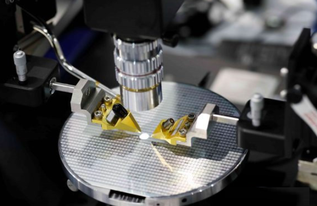
CP(Chip Probing):Test the wafer directly, and the test object is for each Die in the whole wafer, the purpose is to ensure that each Die in the whole wafer can basically meet the device characteristics or design specifications, usually including the verification for voltage, current, timing and function, It can be used to test the level of manufacturing process in fab plants.
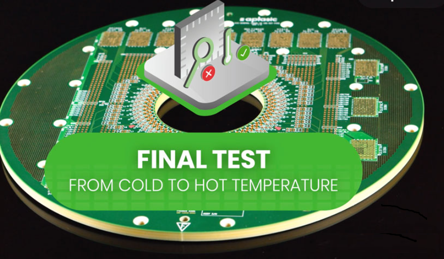
FT(FinalTest):It's the last intercept before the chip leaves the factory. The test object is for the encapsulated chip, which will be encapsulated after CP test and then FT test after encapsulation. It can be used to test the technical level of the packaging plant.
CP for the wafer, if the bad Die does not need to do packaging, saving the cost of packaging and substrate costs.
After the CP test is completed, chip failure will be introduced in the packaging process, so FT is also needed to remove the failed chip.
Yield: The yield of the chip is related to the process, the chip has a certain probability of failure, and the larger the chip, the greater the probability of failure.
IP(Intellectual Property): In integrated circuit design, a complete functional module of a Proven and reusable integrated circuit with a specific function.
IP assortment can be divided into License, Loyalty per toll collection manner
license Authorization License: permit to use this IP, authorization of the IP.
Loyalty royalties: After the user uses the IP, they are charged per chip.
IP is the core component of the chip, such as USB, PCIE, CPU are IP, the whole chip is IP integrated, the chip can do more complex, the core is the reuse of IP. For example, those that make tens of millions of doors, hundreds of millions of doors, are IP reuse can be done.
DUV (Deep Ultraviolet Rays) EUV (Extreme Ultraviolet Rays )
Packaging
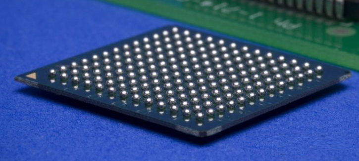
BGA (Ball Grid Array): A type of surface-mounted package in which a number of connected solder balls are arranged on a chip mounted substrate (ball grid array).
ASIC(Application Specific Integrated Circuit): ASIC is a special chip, which is a general term for a chip that is specially customized for a specific need. For example, dedicated audio and video processors, and at present, many dedicated AI chip industry can be regarded as a kind of ASIC.
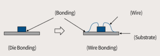
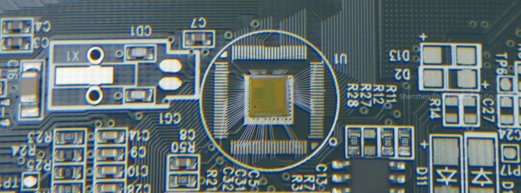
Wirebonding: Wire Bonding(press welding, also known as binding, bonding, wire welding) refers to the use of metal wire (gold wire, aluminum wire...etc.), the use of hot pressing or ultrasonic energy to complete the connection of the internal wiring of the solid-state circuit, that is, the connection between the chip and the circuit or the lead frame.
Die bound:
Flipchip: A tin lead ball is deposited on the I/Opad, and then the chip is turned over and heated using the molten tin lead ball combined with the ceramic substrate.
COB (chip-on-board):On-board chip packaging is to attach the bare chip to the PCB with conductive or non-conductive adhesive, and then perform lead bonding to achieve its electrical connection, and wrap the chip and bond lead with adhesive.
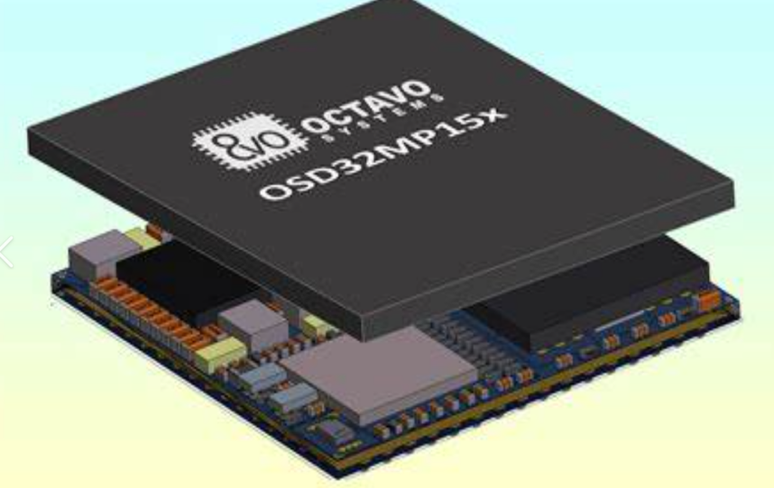
SOC(System On Chip): Is to put the CPU, bus, peripherals...etc., into a chip internal implementation. For example, a mobile phone processor is a complex SOC chip.
SIP (System In Package): SiP package is the raw chip with different functions, including CPU, GPU, memory...etc. integrated in a package body, so as to achieve a whole chip system.
SOP(Small Outline Package):A small external package of IC packages in which the leads are pulled in both directions
DAF (Die Attach Film): Wafer bonding film bonding technology
CMOS (Complementary Metal Oxide Semiconductor): Complementary metal oxide semiconductor. It refers to a technology used to make large-scale integrated circuit chips, or chips made using this technology, which is a piece of RAM chip that can be read and written on a computer motherboard. Because of the read-write characteristics, it is used to save the BIOS data after the computer hardware parameters is setted on the computer motherboard, and this chip is only used for storing data.
JEDEC (Joint Electron Device Engineering Council Standards): U.S. standard specifications for package dimension.
Fountyl Technologies PTE Ltd, is focusing on semiconductor manufacturing industry, main products include: Pin chuck, porous ceramic chuck, ceramic end effector, ceramic square beam, ceramic spindle, welcome to contact and negotiation!