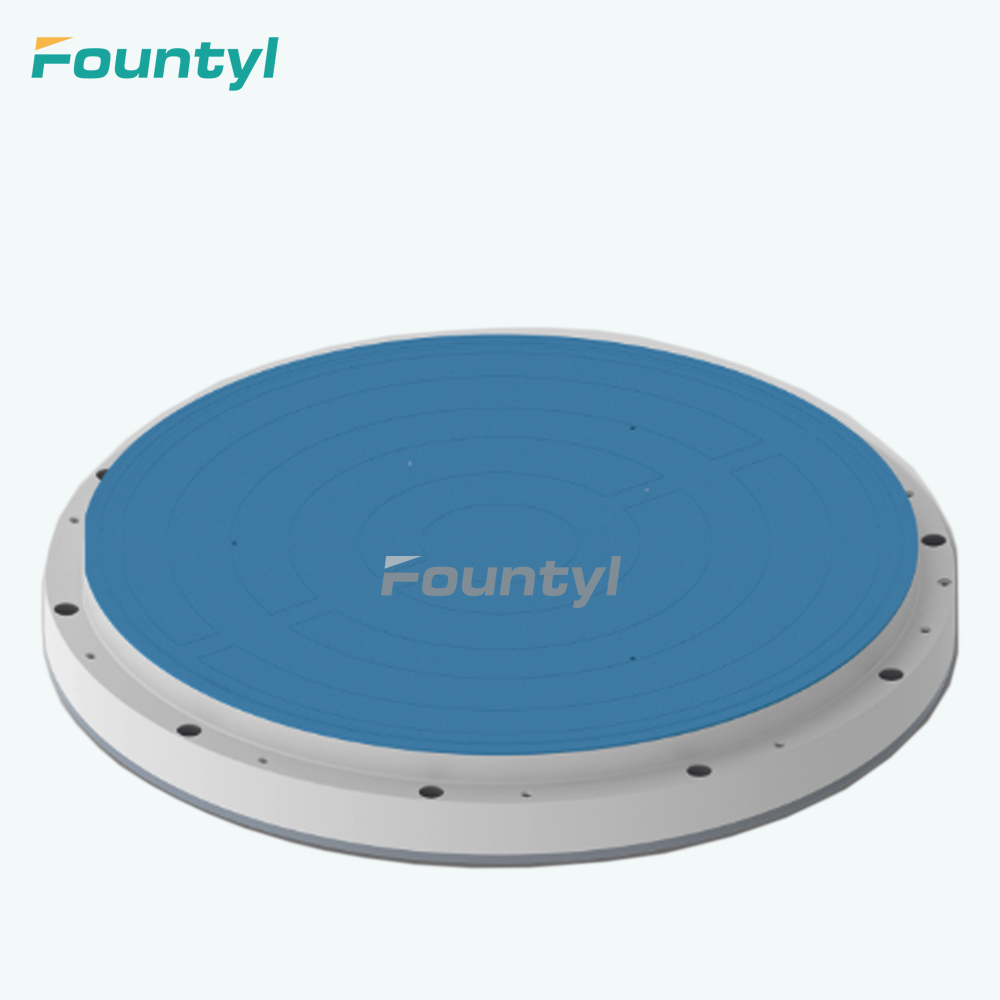
Features
Compatibility | Customization | High-Density | High Structural Strength | Fast Delivery Time | Cost-effective
Applications
Lon-implantation | Thin Film | Etch | Process Development | Equipment Design
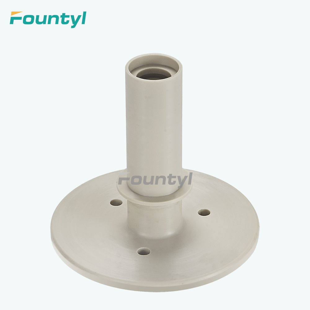
Design and Manufacture
12 inch Fab delivered to verify the actual performance, provide regeneration and repair, and verify the development and design.
With the process equipment and process technology development of semiconductor and integrated circuit, the traditional electrostatic chucks using organic polymer materials, metal oxides and ceramic materials as dielectrics are not fully compatible with such materials as silicon wafers, sapphire and silicon carbide. Therefore, electrostatic chucks compatible with the first, second and third generation semiconductor wafer grippers will gradually develop.
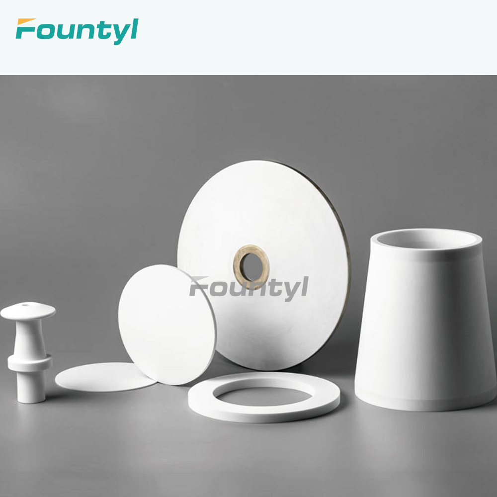
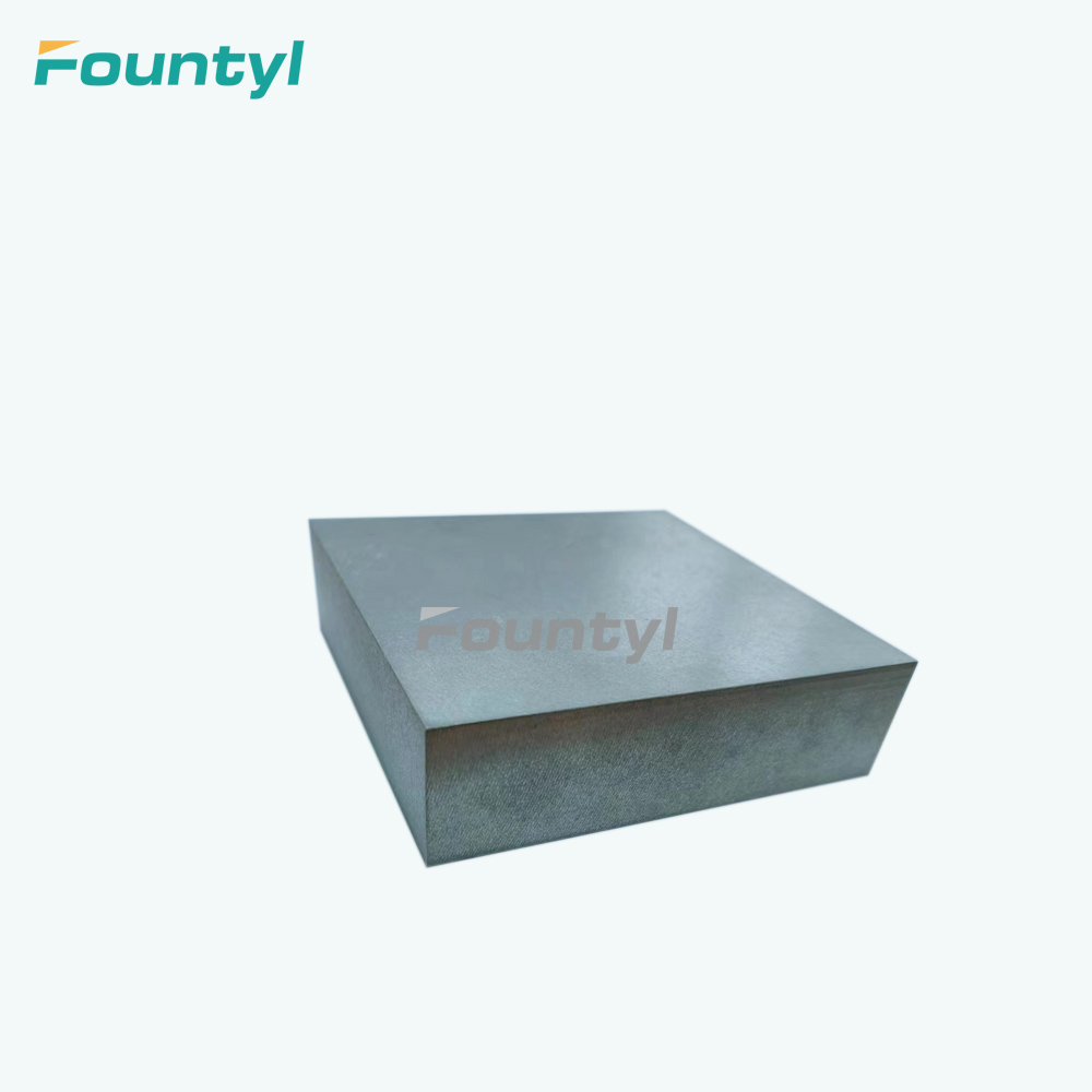
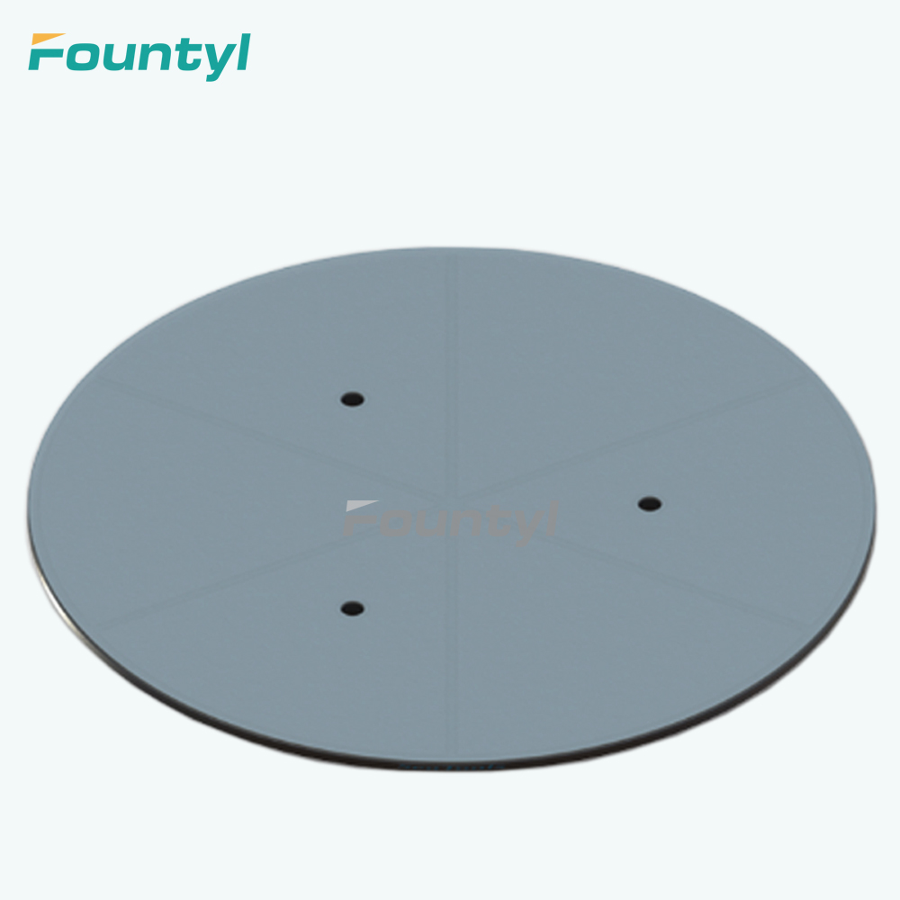
Polymer Electrostatic Chuck / Heater
Polymer dielectric material (Polymer) is currently the most widely used electrostatic chuck material, its preparation process is also the most mature, polymer dielectric material after polymer modification treatment, electrical, mechanical, temperature resistance, halogen resistance properties will be greatly improved. The dielectric material is patterned by other integrated operations, and then layered by multistage vacuum heavy load, and a dense dielectric insulation layer is formed between the internal electrodes.
Polymer Electrostatic Chuck
The polymer modification technology is used to achieve higher bulk resistivity and relative dielectric constant, and obtain more stable clamping force.
High density dielectric materials can reduce the risk of particulate matter and reduce ion mobility.
The diversity of clamping objects can be compatible with the clamping of wafers of different materials.
Excellent corrosion resistance in halogen and plasma atmospheres.
High cost performance, short acceptance period, suitable for product process development and new equipment development verification.
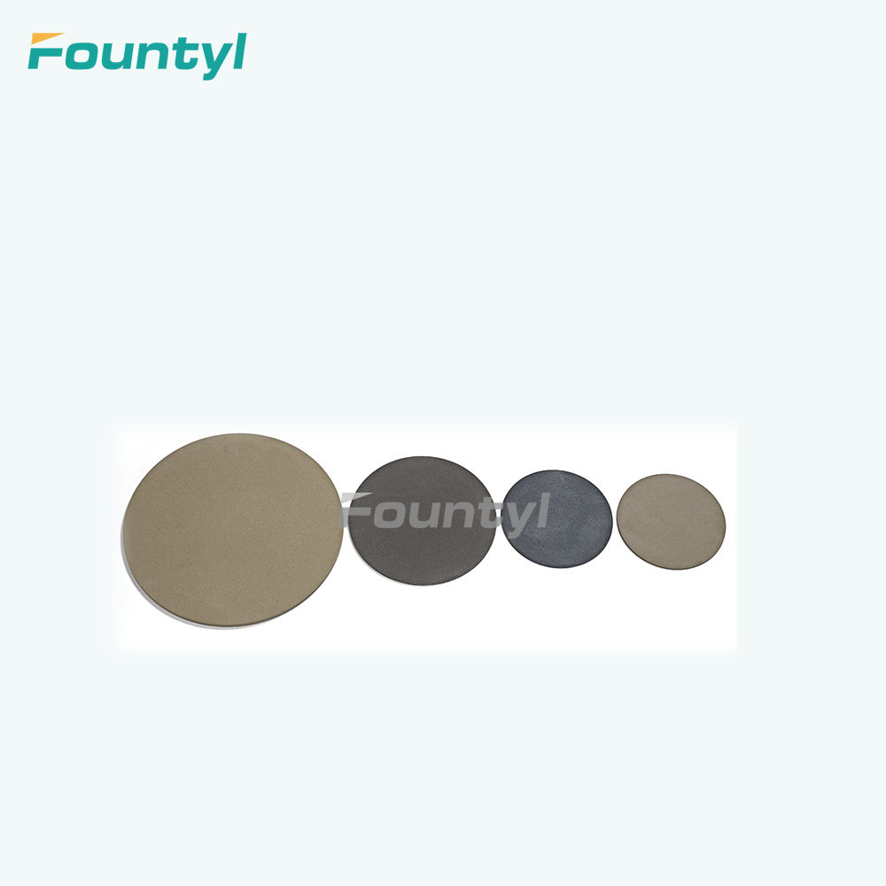
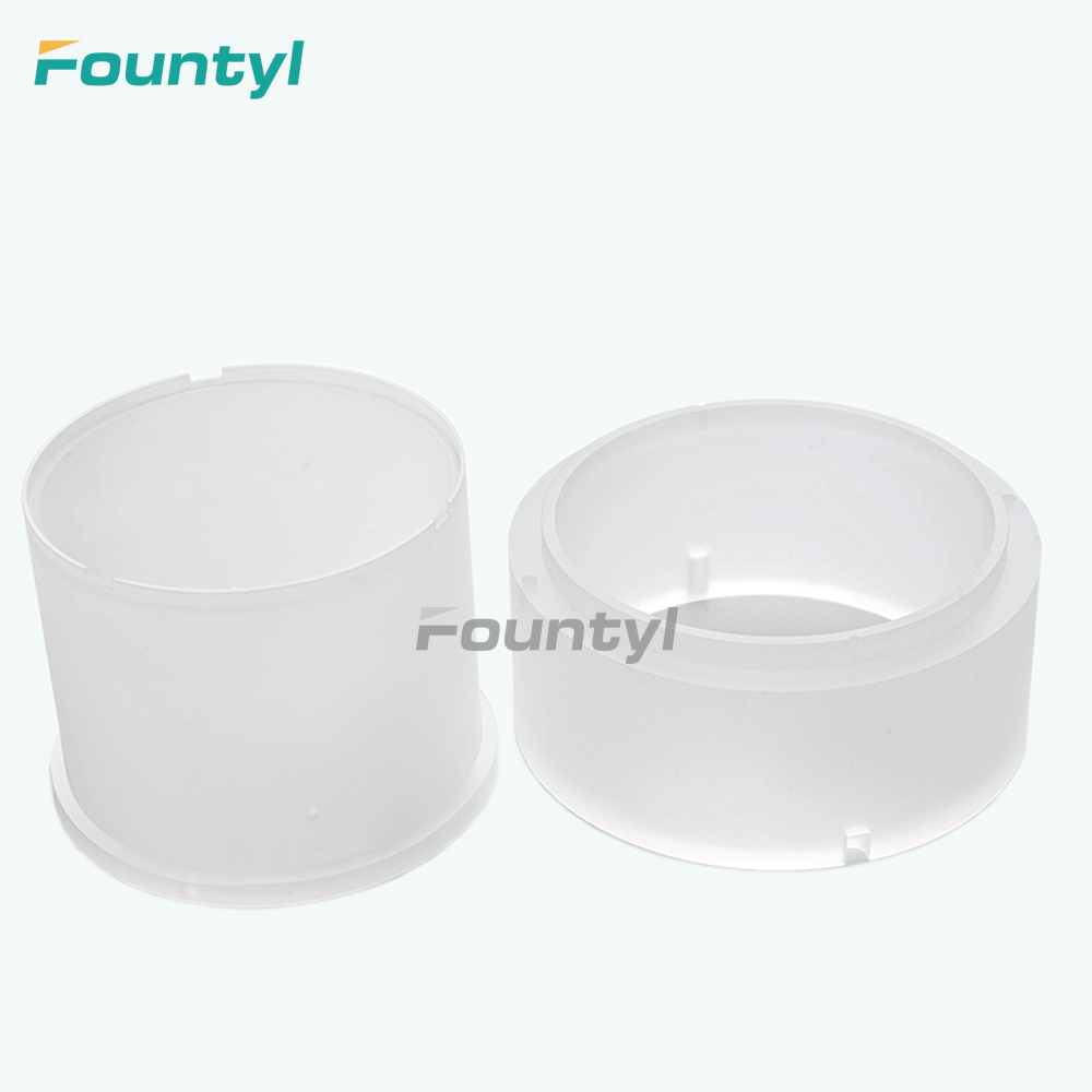
Al₂O₃ Electrostatic Chuck
The volume resistivity is controlled by coagulation ceramic technology and co-firing process to obtain a longer holding force.
The internal structure of high temperature sintering is dense and the crystal structure is stable, and the holding capacity of a larger temperature interval can be obtained.
Integrated co-firing molding reduces ion migration.
Lasting operation in plasma halogen vacuum atmosphere.