

Porous silicon carbide chuck
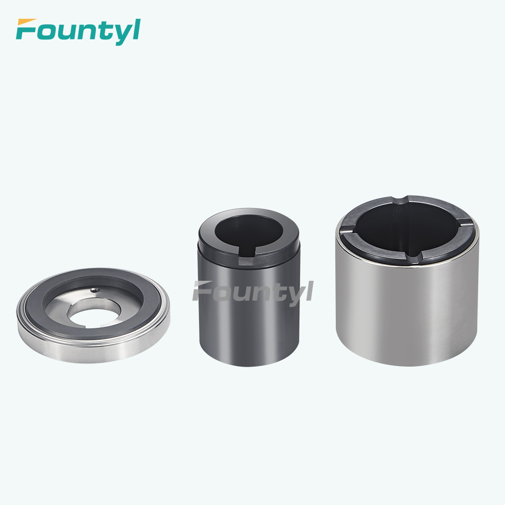
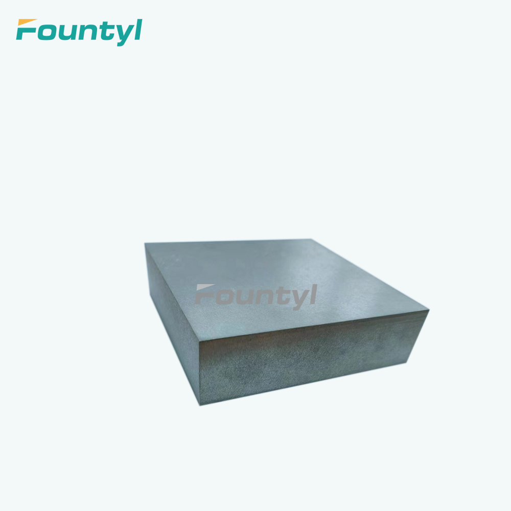
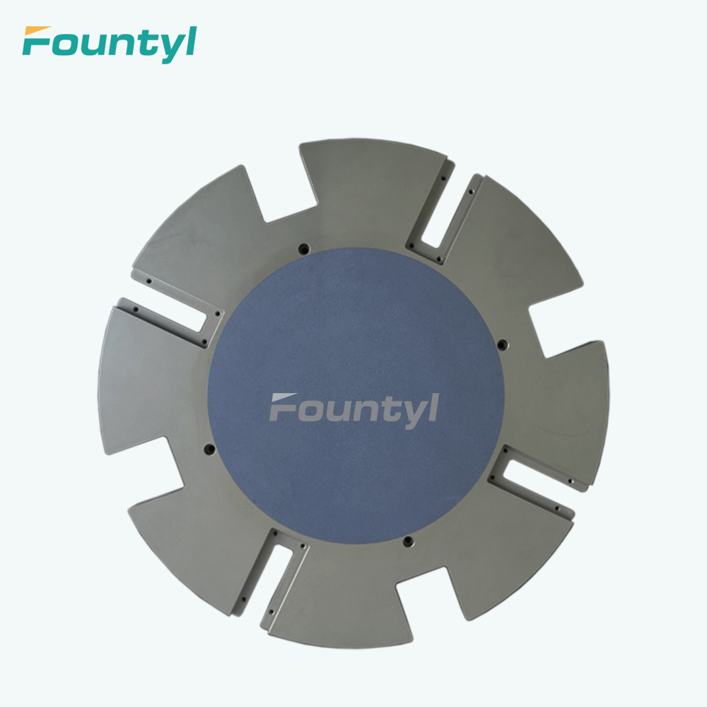
Porous silicon carbide chuck(reaction bonded SiC chuck, sintered silicon carbide chuck)
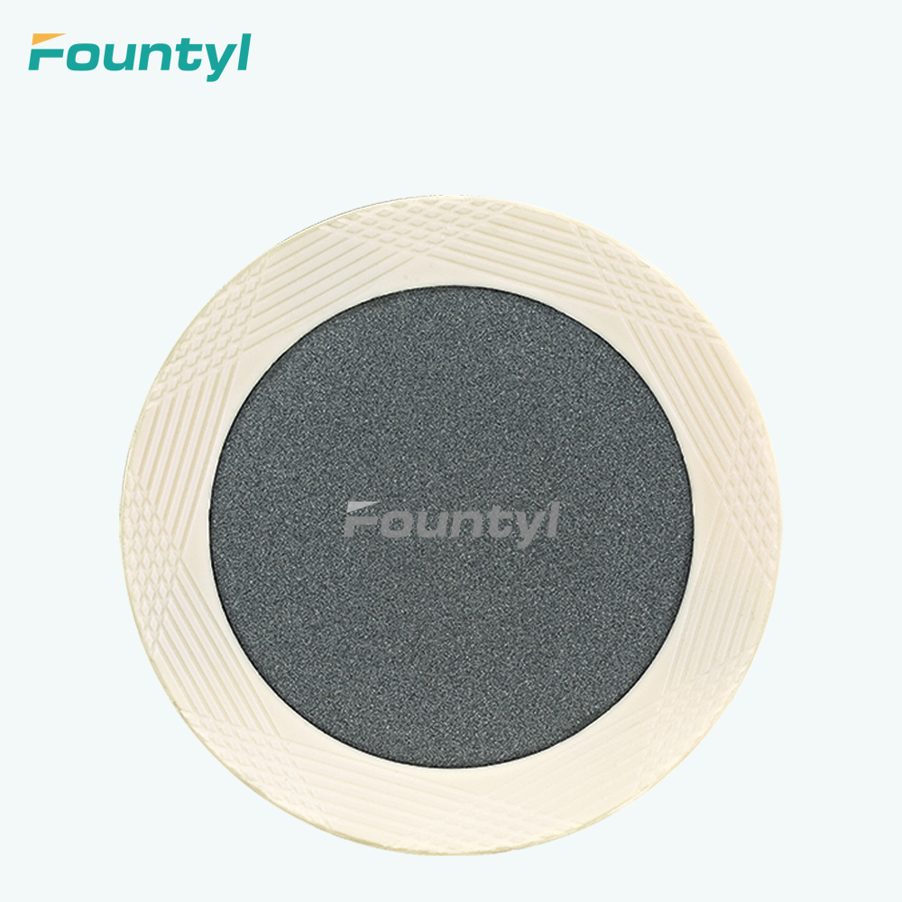
Ceramic vacuum chuck features
Strong permeability: uniform air permeability and water permeability, to ensure the uniform force and tightly adsorption of the silicon wafer in the grinding process without slide.
Dense and uniform structure: Adoption of micro-porous ceramic material with the dense and uniform structure, which is not easy to adsorb silicon dust, and the chuck is easy to be cleaned.
High strength: no deformation during grinding, to ensure that the silicon wafer is evenly stressed at each point when grinding, and it is not easy to occur the phenomena of edge collapse, debris.
Long life: the surface shape retention is good, the dressing cycle is long and the dressing amount is small, so it has a high life.
Easy dressing: there will be no cracking, fragmentation, threshing phenomena when dressing.
Lightweight: Due to the internal structure of pores, the specific gravity coefficient is 1.6-2.8.
High insulation: insulating material, eliminate static electricity.
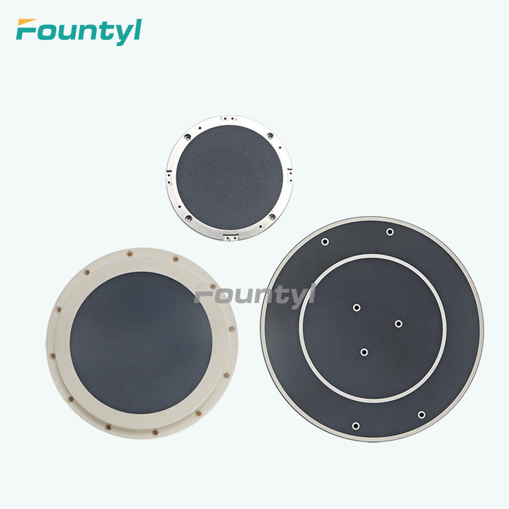
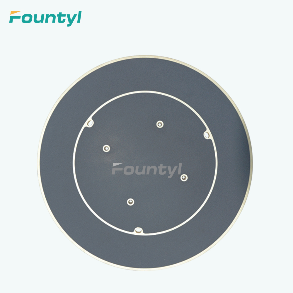
Accuracy Control
| category | Base material | Adsorption surface material | Size | Flatness | depth of parallelism |
| Porous chuck | Aluminium Alloy | Porous SIC | ≤12μm | ≤15μm | ≤20μm |
| Stainless steel | ≤10μm | ≤15μm | |||
| Alumina | ≤5μm | ≤8μm | |||
| Silicon Carbide | ≤3μm | ≤8μm | |||
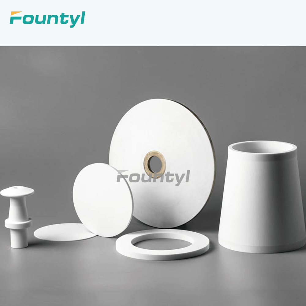
| The porous ceramic chuck has a complete range of specifications and sizes, which can be used in the 3-inch line, 4-inch line, 5-inch line, 6-inch line, 8-inch line and 12-inch line, and can be customized according to the specifications and sizes you need. | |||||
| The maximum size of the current case is :1600*1600m, thickness is 50mm; | |||||
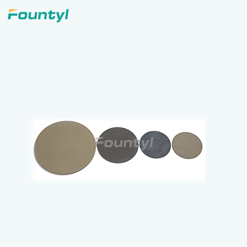
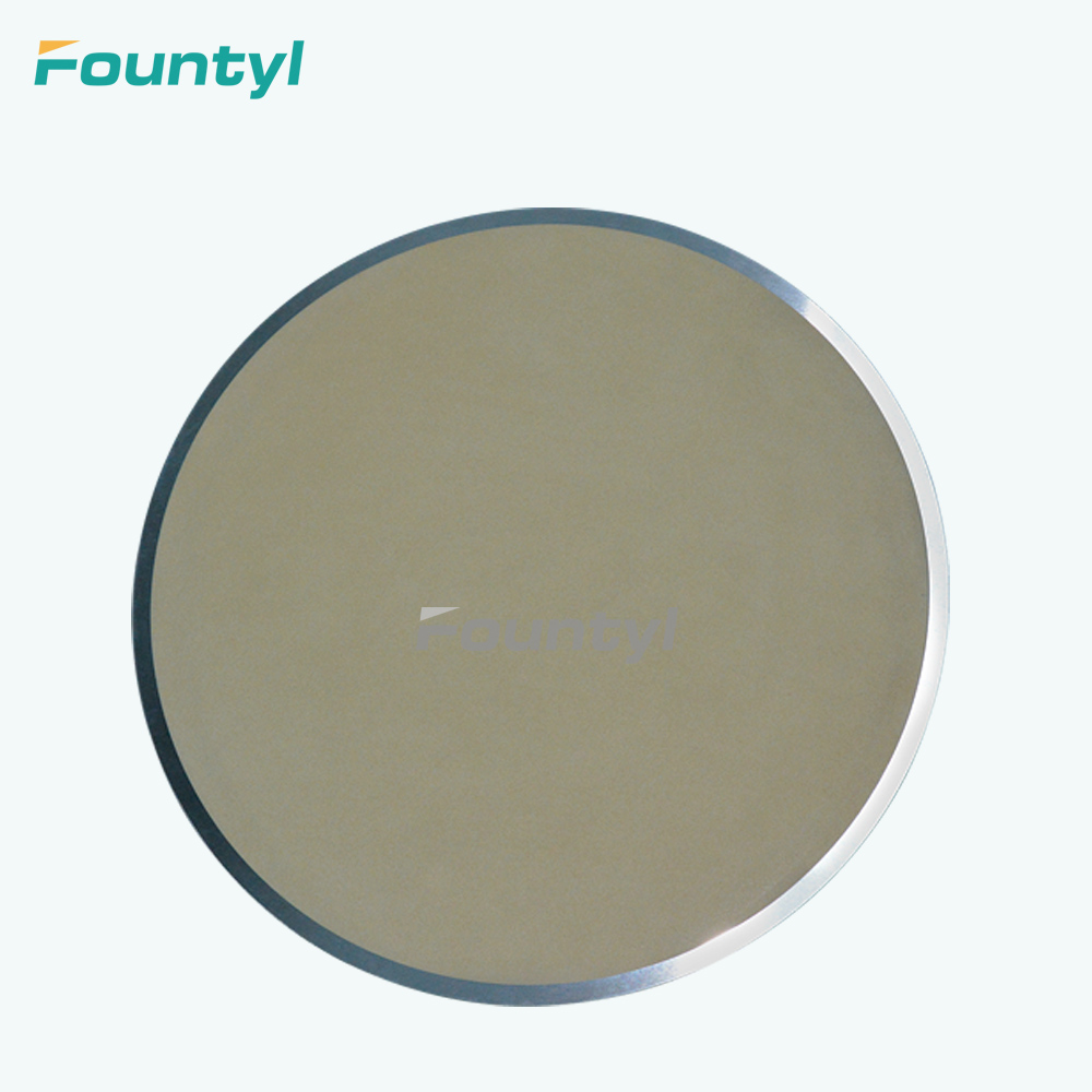
Porous ceramic material characteristics:
Main ingredients: alumina Color: black, iron gray
Alumina content: 92% Moisture content: 0%
Aperture: 2~30um Porosity: 35~40%
Bending strength :6kgf/cm2 (Mpa) Volume ratio: 2.28g/cm3
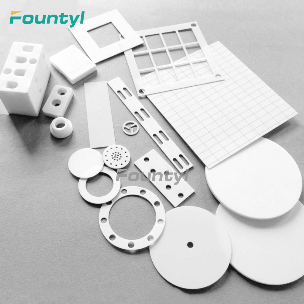
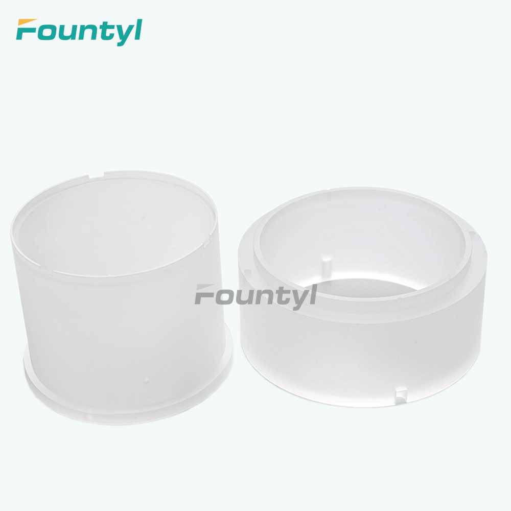
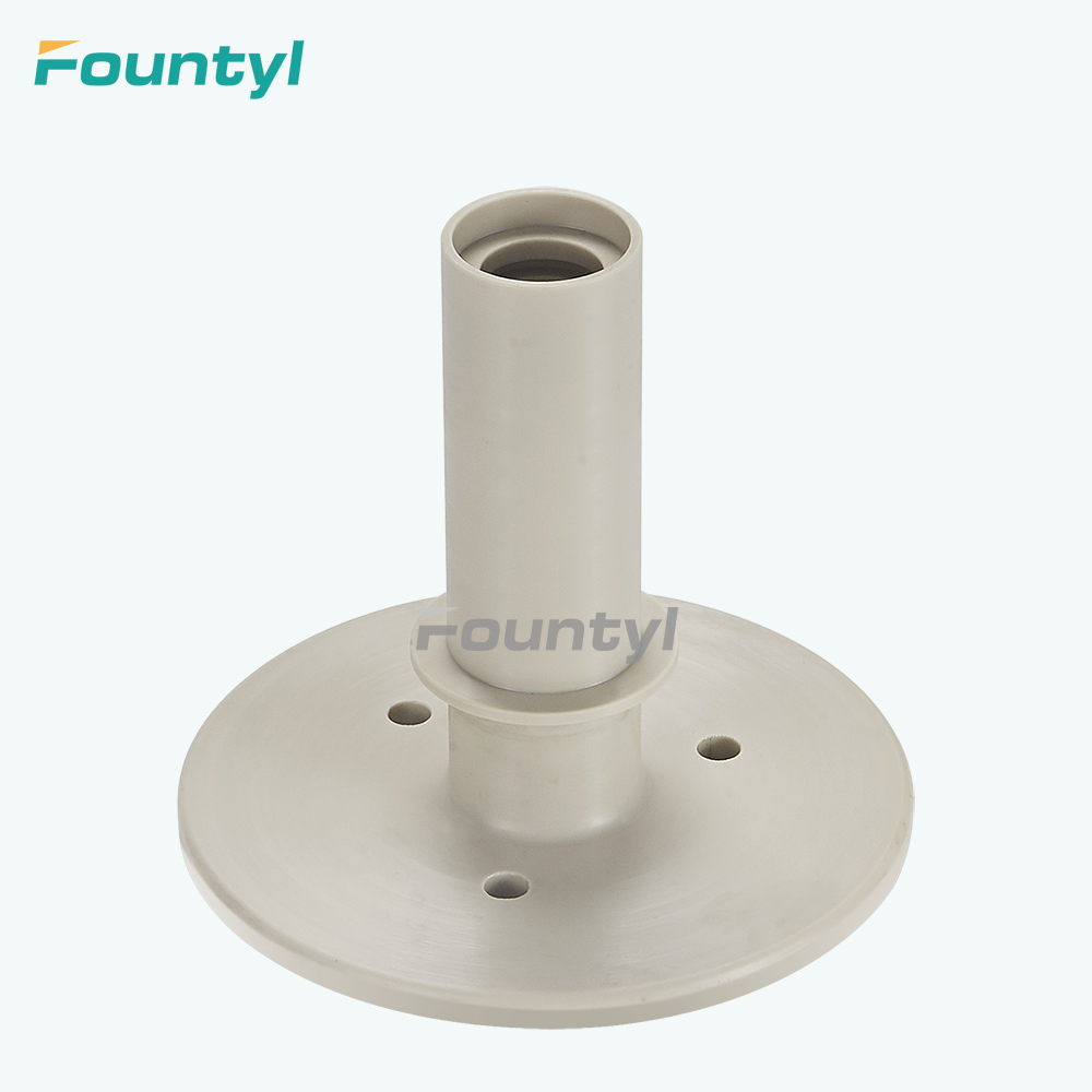
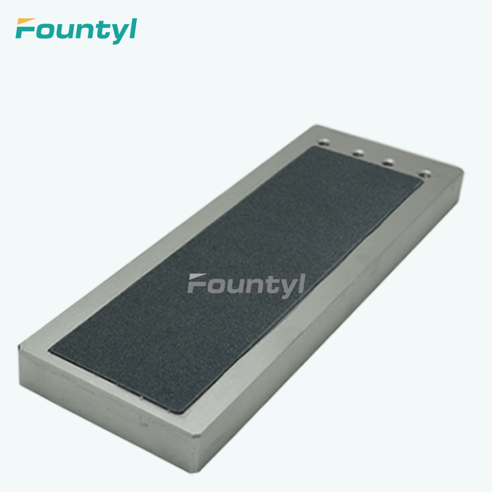
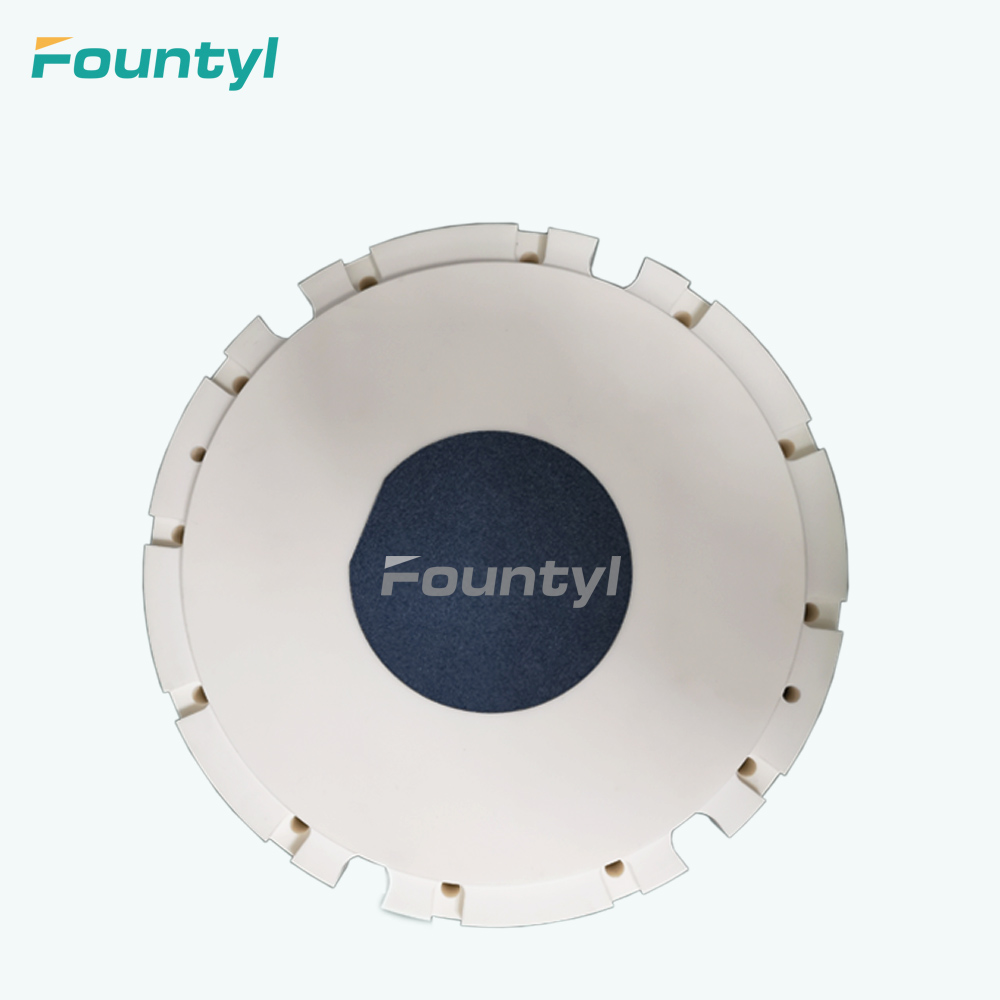
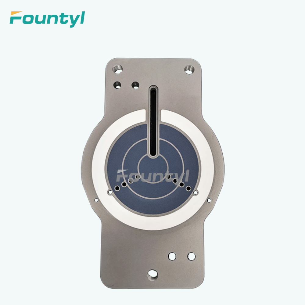
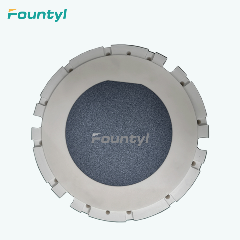
Ceramic chuck type
According to the usage, Ceramic chuck are divided into :
Thinning machine equipped with: abrasive disc chuck, silicon wafer, sapphire substrate and other thinning;
Cutting machine is equipped with: scribing chuck, silicon wafer, semiconductor compound wafer and other cutting;
Cleaning machine equipped with: cleaning chuck;
Film removing machine is equipped with: film removing chuck;
Laminating machine equipped with: laminating chuck;
Printing machine equipped with: printing chuck.
Quality assurance
Fountyl has many years of technical experience on engineering ceramic precision and ultra-precision processing and manufacturing, a variety of physical and chemical analysis instruments and geometric measurement instruments, to ensure the stability of production and consistency of product for ceramic chuck.
Product Application
Porous chuck (adsorption working table) is a component used in the semiconductor manufacturing stage and assembled on a scribing machine or inspection device. It is a product that can use the porous structure and negative pressure of the surface of the workbench to keep the thin silicon wafer flat. The scribing machine cuts the silicon wafer with the width about 20μm, so the requirement to flatness and parallelism of the wafer adsorption surface are very high. According to their respective characteristics, different pore structures have different application ranges, such as microporous ceramics with large specific surface area and small pore size, usually used in bacterial filtration and microbial fixation fields; Mesoporous ceramics with their specific diameter distribution are often used in separation, adsorption catalysis fields. Macroporous ceramics are usually suitable for rough filtration of substances with a large content and large size.