


News

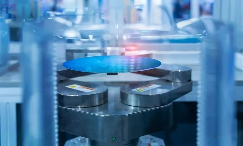
Common wafer development methods
The wafer development process is an essential step in the lithography process and has undergone decades of innovation and advancement. So how many common development methods are there? What are the types of developer? What is the development mechanism? What are the main controlling factors for development?
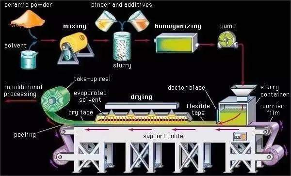
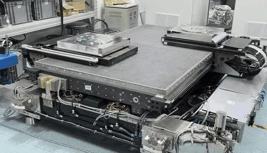
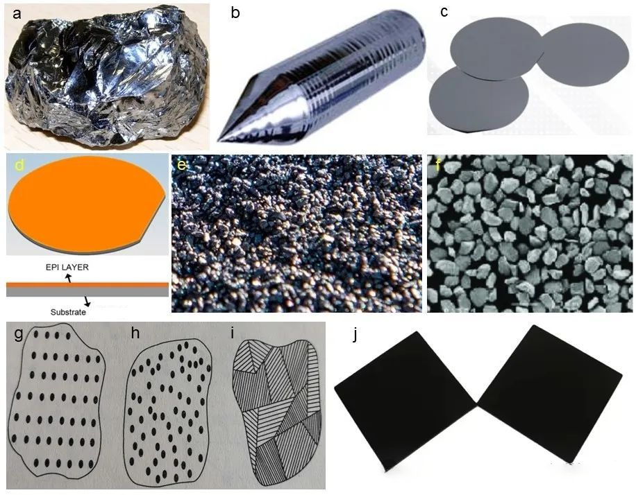
Molding process and technology development trend of special ceramics
Because of special ceramics with high temperature resistance, wear resistance, corrosion resistance, high hardness, high precision and other advantages that metals and plastics do not have, and in the fields of electronics, superconductivity, optics, biology, magnetism, energy storage and so on, become the "material black gold" in the upstream of many high-tech industrial chain.
Preparation of ceramic slurry: ball milling
Ball milling is a grinding method, mainly through the ball as a medium, the use of impact, extrusion and friction to achieve the crushing of materials.
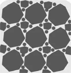
Ceramic formulation: Particle size
The formula of ceramic refers to that under the configuration of raw materials of different shapes and different particle sizes, the physical and chemical properties of the finished products under the corresponding ceramic production process conditions and firing conditions meet the requirements.
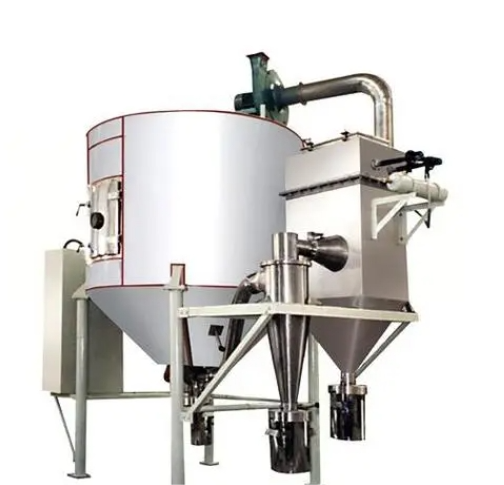
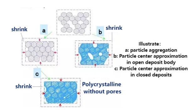
Spray granulation of ceramic powder
Spray granulation of ceramic powder is a special granulation method, which is mainly used for the treatment of ceramic powder.
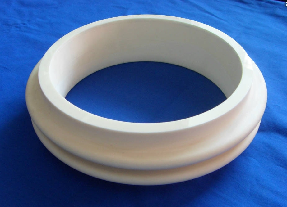
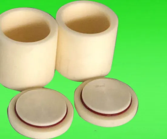
Functional ceramics: key materials in the field of advanced modern science and technology
Functional ceramics is a kind of advanced material which utilizes light, heat, force, sound, magnetism, electricity and other direct effects and coupling effects.

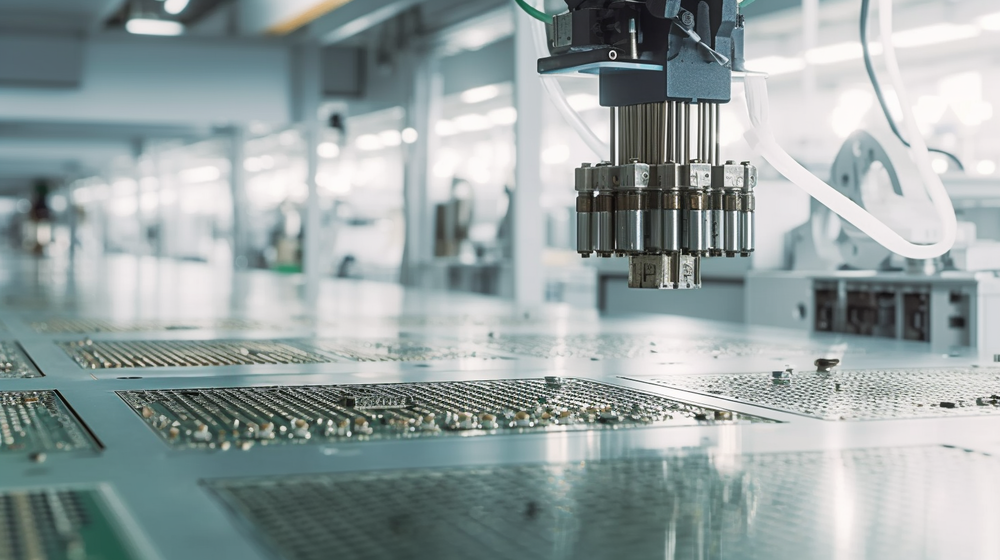
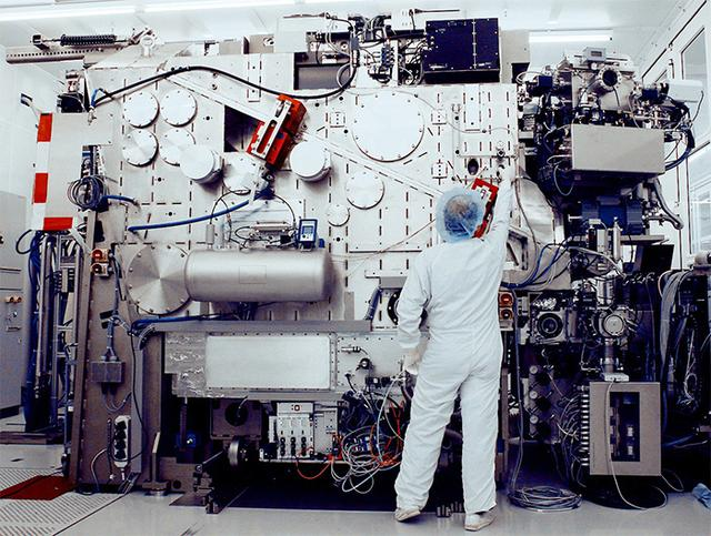
An essential element in chip manufacturing- Plasma
Plasma was first discovered by William Crookes in 1879 and named "plasma" by Irving Langmuir in 1929. The application of plasma in chip manufacturing is very common and important, it can be said that without plasma, chip production would not be possible. Plasma is almost always involved in dry etching, PVD, CVD, wafer surface modification and lithography.
A necessary element in chip manufacturing - vacuum
Vacuum is very important in semiconductor manufacturing, in the semiconductor industry, the vacuum environment is used in various processes, It includes Physical Vapor Deposition (PVD), Chemical Vapor Deposition (CVD), and Atomic Layer Deposition (Atomic Layer Deposition). ALD, Ion Implantation, Plasma Etching, and so on.
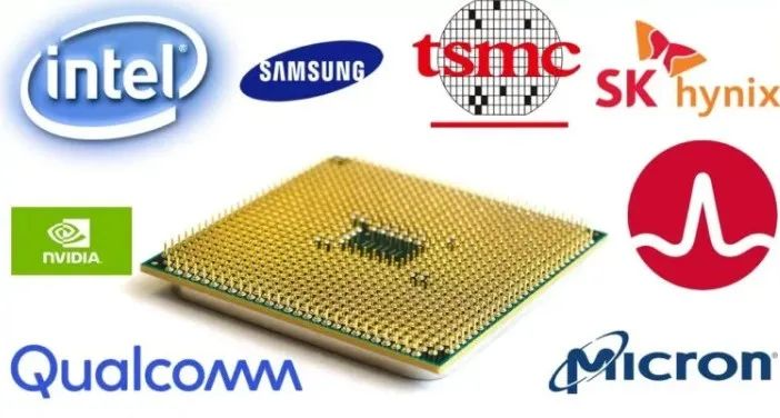
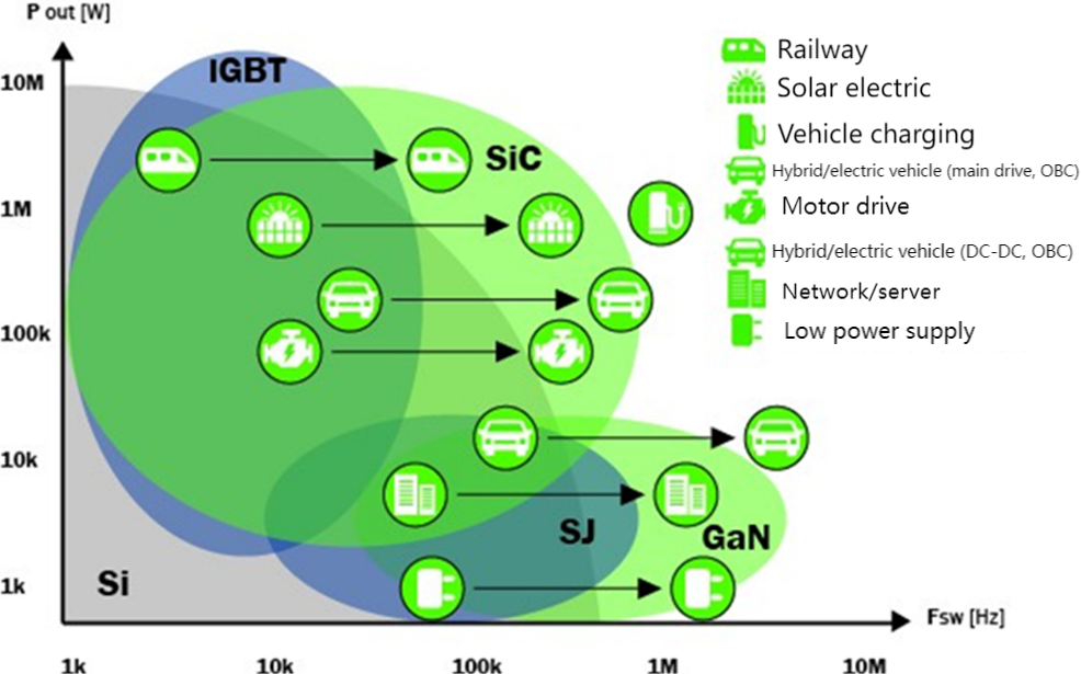
The world's Top10 semiconductor companies, and its main technical strength
Here are the top 10 semiconductor companies in the world by market capitalization and sales revenue.