


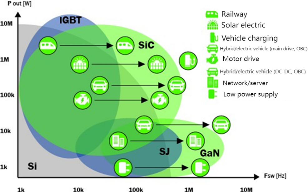
News
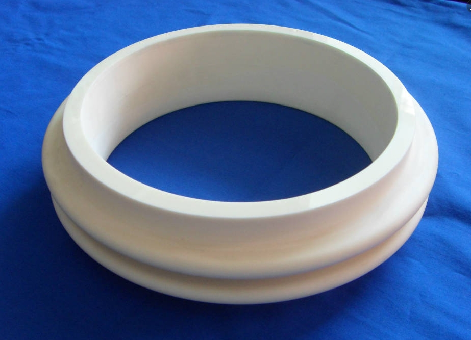
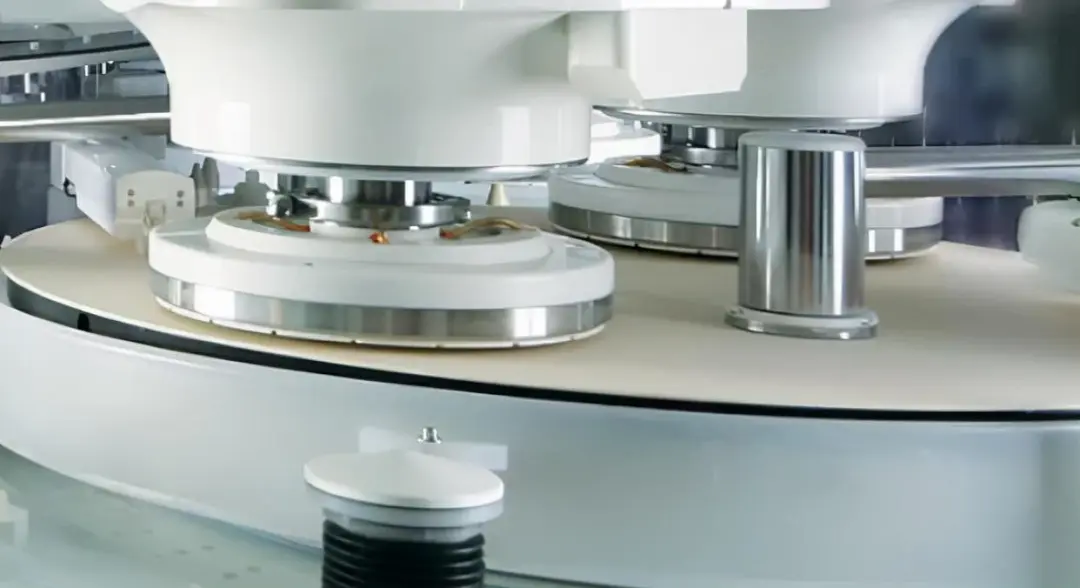
Ceramic electrostatic chuck: How is this "stuck neck" semiconductor component produced?
In order to meet the growing and diversified trend of system demand, wafer-level packaging technology is constantly breaking through the direction of high density, ultra-thin, ultra-small and higher performance, at the same time, the problem of ultra-thin device wafer clamping has also put forward new demands and challenges.
Demand and application of alumina powder in electronic manufacturing, semiconductor, new energy and other high-end fields
Fine alumina powder through the precision processing of industrial raw materials to adapt to the application needs of different industries.
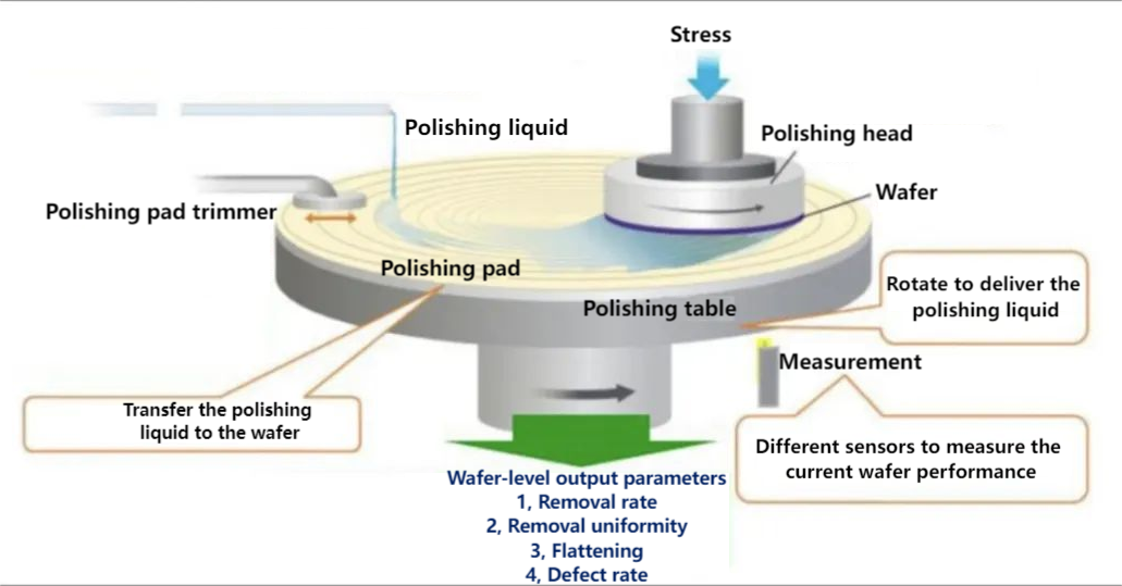
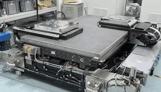
Master mirror grinder for CMP device semiconductors
CMP (Chemical Mechanical Polishing) technology is a key process for achieving global uniform and flat wafer surfaces in semiconductor manufacturing
The most complete summary of the ten structural ceramic forming processes
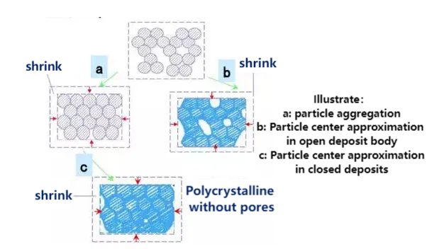
Ceramic forming is an important part of the ceramic preparation process, the forming technology to a large extent determines the uniformity of the body and the ability to prepare complex shaped parts, and directly affects the reliability of the material and the cost of the final ceramic parts.
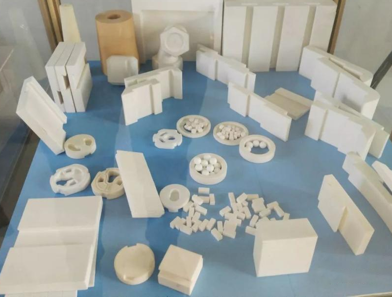
Detailed classification of ceramic materials
Ceramic materials refer to a class of inorganic non-metallic materials made of natural or synthetic compounds by forming and sintering at high temperature. It has the advantages of high melting point, high hardness, high wear resistance and oxidation resistance. Can be used as structural materials, tool materials, because ceramics also have some special properties, but also as a functional material.
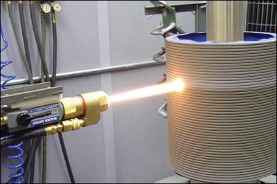
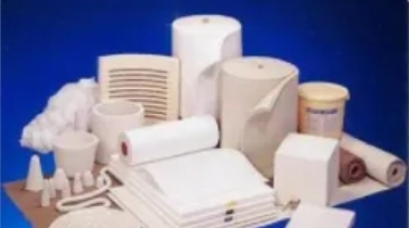
Progress in preparation and application of ceramic coatings
Ceramic coating is a general term for a class of inorganic non-metallic coating, which not only maintains the advantages of high temperature resistance, wear resistance and corrosion resistance of traditional ceramic materials, but also maintains the structural strength of the base material.
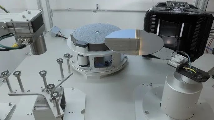
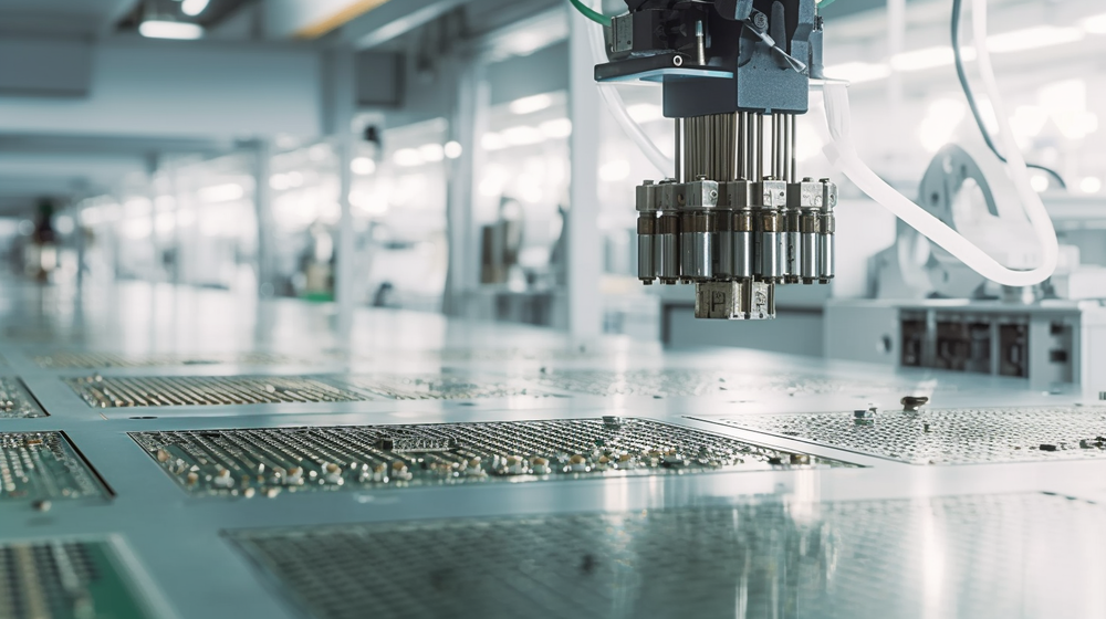
Common wafer adsorption technology
Wafer adsorption technology is a seemingly trivial but crucial link. Whether etched, deposited or lithographed, wafers must be stably and precisely fixed in the right position to ensure efficient chip production
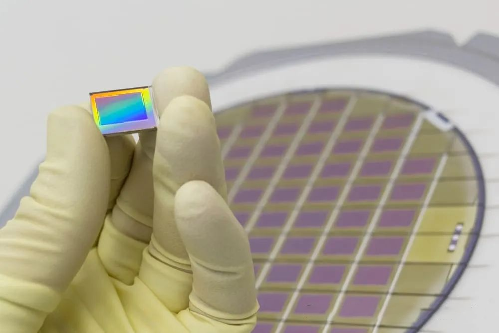
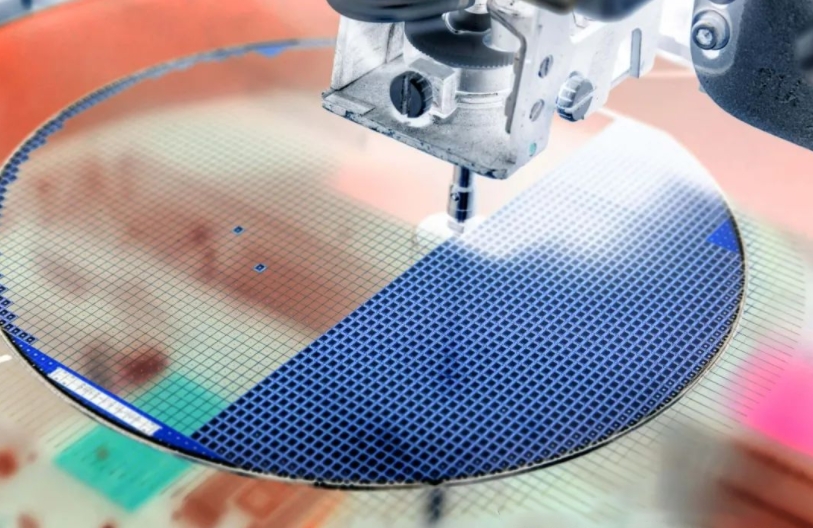
What are the methods of wafer scribing?
Wafer slicing (cutting) refers to the process of cutting a single wafer into multiple independent chips (" dies ").
X-ray applications in chip manufacturing
X-rays are widely used in production and life, and the importance of semiconductor manufacturing is self-evident. Today, let's talk about the application of X-rays in semiconductor manufacturing.
Summary of common semiconductor manufacturing processes
Semiconductor manufacturing refers to the process of machining a complete chip that can achieve a specific function on a wafer through a series of complex steps.