


News

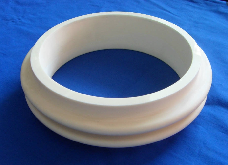
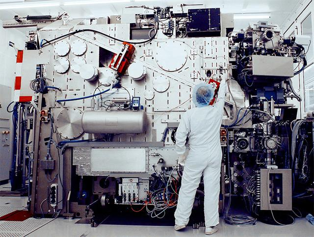
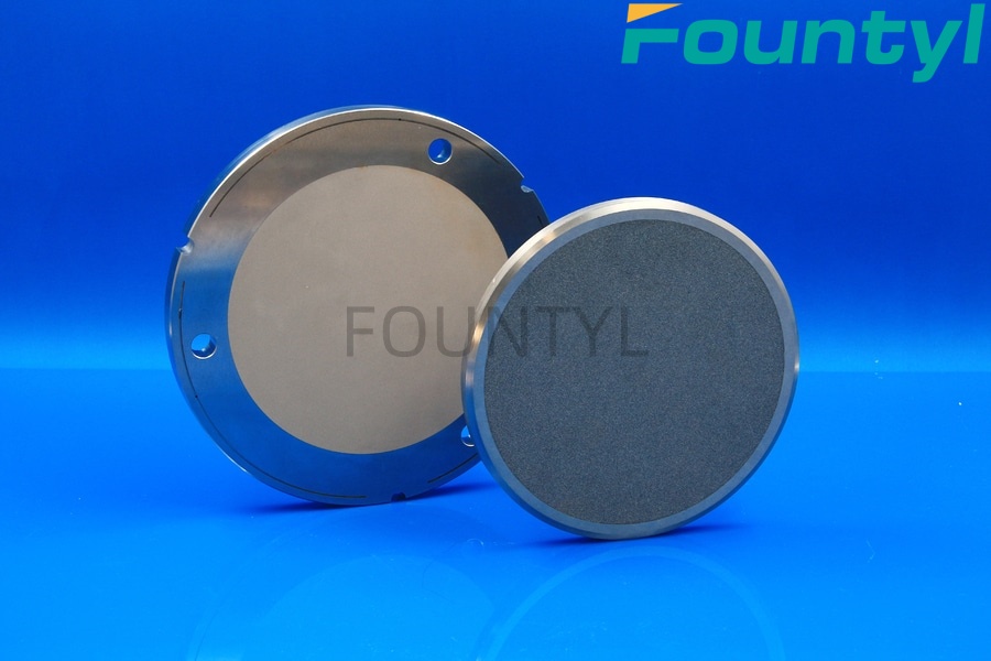
The key point and product characteristics of microporous ceramic vacuum chuck
We have developed novel porous ceramics whose pore sizes can be made in the range of less than 1 micron to hundreds of microns. Air is drawn out through tiny pores, and the processed material is pressed against the ceramic surface. True vacuum fixation.
Semiconductor equipment market cautiously optimistic, there are still bright spots
Recently, the world's top four semiconductor equipment manufacturers have successively announced the 2023 annual report or the latest quarterly report in 2024. Around the growth fulcrum of semiconductor equipment in 2024, technology priorities, and macro situation, the head companies have drawn these priorities.
History of the world's five largest semiconductor companies
Semiconductor industry chain is too large, semiconductor giant companies are usually through continuous acquisition or merger to enrich their product lines, so as to provide customers with a complete set of solutions.

The three major foundry giants launched the 2nm battle
The world's leading semiconductor companies are racing to produce 2nm chips to power the next generation of smartphones, data centers and artificial intelligence (AI).

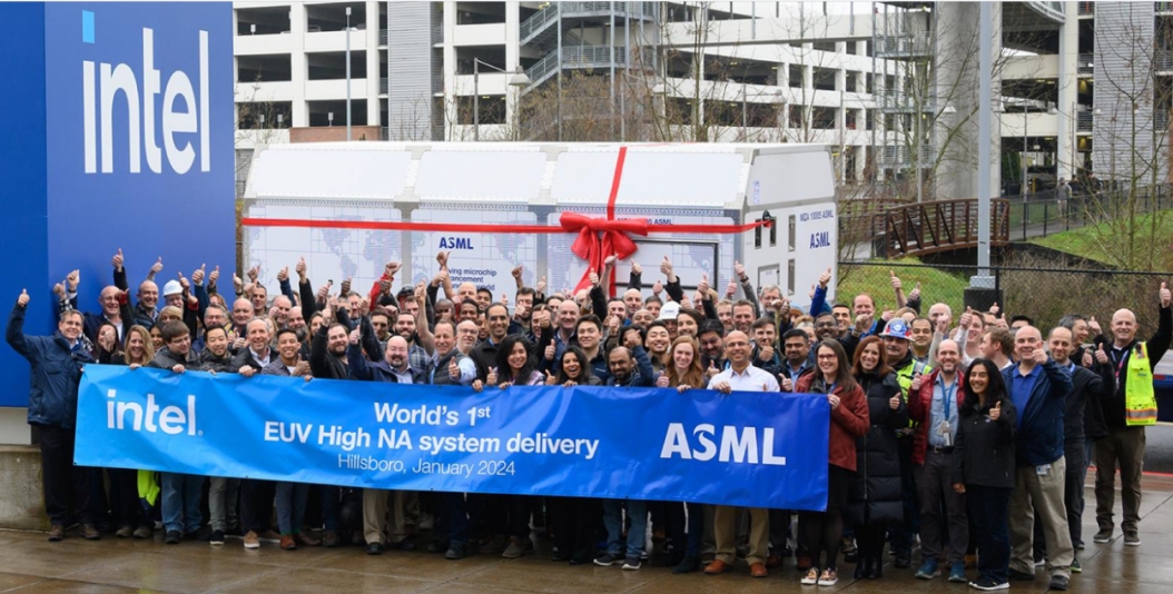
The world's top five semiconductor equipment brewing big changes
As the core equipment of chip manufacturing, EUV lithography machine has attracted much attention, and the importance of ASML has become more and more prominent, and in this wave, the pattern of semiconductor equipment market is also quietly changing
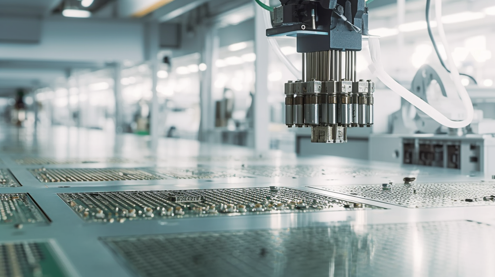
What is the use of silicon oxide (SiO2) film?
The entire semiconductor manufacturing process is very common and indispensable, what is it used for?
How are wafers stored and shipped?
What are the special requirements for the storage and transportation of wafers after they have completed all the processes in the fab? Do special environmental packaging be required?
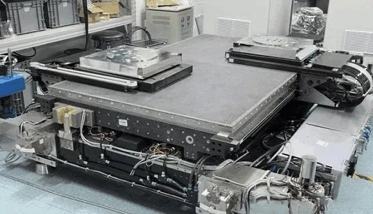
Common wafer slicing methods
Wafer scribing, as a key step in semiconductor manufacturing, directly affects the quality and output of the chip.
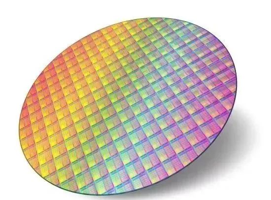
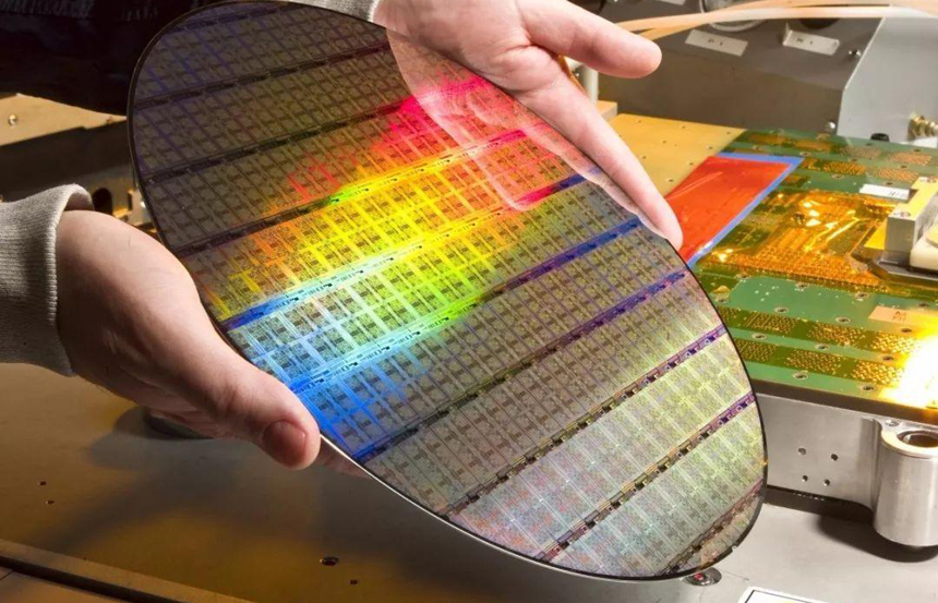
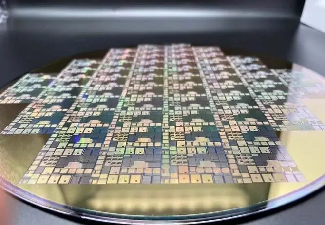
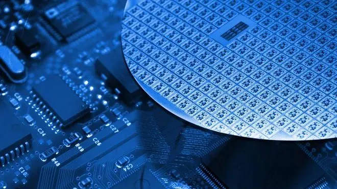
Why are chips square and wafers round?
In the public impression, the wafer is a thin, round high-purity silicon wafer, and on this high-purity silicon wafer can be processed to produce a variety of circuit component structures, so that it becomes an integrated circuit product with specific electrical functions.
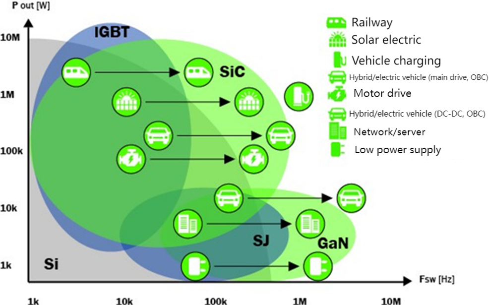
Third generation semiconductor silicon carbide emerging, can be applied to the new wafer cutting process?
With the rapid development of information technology and the growing demand for high-efficiency electronic devices, the third-generation semiconductor materials represented by silicon carbide (SiC) are gradually emerging with their advantages in band gap width, dielectric constant, thermal conductivity and maximum operating temperature.