


News

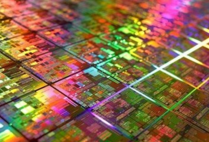
Japanese companies monopolize the EUV photoresist supply market
Although there will be more photoresist manufacturers for EUV lithography. But at the moment the market is dominated by Japanese companies.
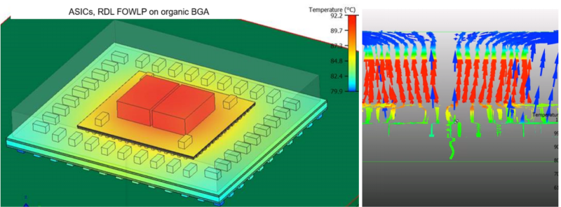
How to solve the chip package heat dissipation problem
Placing multiple chips side-by-side in the same package can mitigate thermal issues, but as companies delve further into chip stacking and denser packages to improve performance and reduce power, they're battling a new set of heat-related issues.
How can the semiconductor industry contribute to the goal of "green and low-carbon"?
The development of semiconductor technology is an important driving force for building a green and low-carbon society. At the same time, the semiconductor industry itself is actively achieving green and low-carbon, and is an active practitioner of the strategic goal of carbon neutrality.
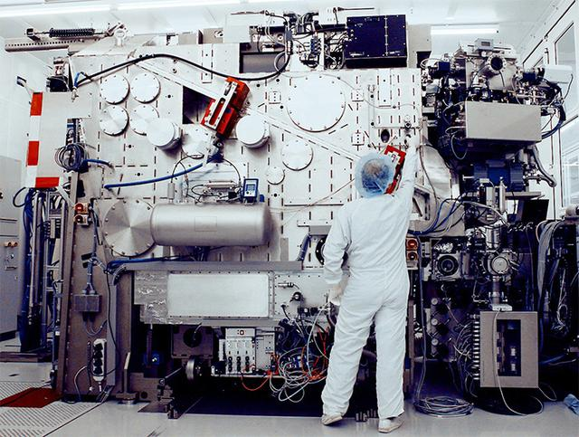
Global wafer shortage and countermeasures
In recent years, the global supply and demand of wafers is unbalanced, and the shortage of 200mm wafers will continue for several years.

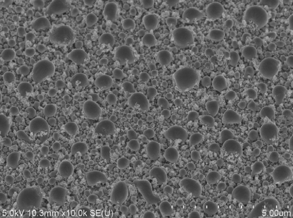
Progress has been made in the study of 8-inch silicon carbide single crystals
The characteristics of high-quality crystal quality of SiC epitaxial layer make the epitaxial layer should have a crystal structure of high purity and low defect density to ensure the reliability of SiC components.
Improved gallium nitride substrate thinning technology
Switching to a hydrogen-based plasma ensures high-speed etching of GaN substrates, and engineers at Osaka University in Japan claim to have made a new breakthrough in thinning gallium nitride (GaN) substrates using hydrogen-based plasma.

The South Korean team used IGZO to make artificial intelligence chips
The successful development and application of this new AI semiconductor technology shows great potential to improve the efficiency and accuracy of AI."

The application prospect of nanotechnology is very broad
IEEE experts pointed out that from solar coatings to instant rechargeable batteries, nanotechnology has a broad application prospect
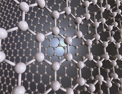
A new breakthrough in semiconductor materials - graphene
Currently, IBM, along with Samsung and the U.S. Air Force and Navy, is funding the research, which is considering the use of graphene in semiconductors and computers.
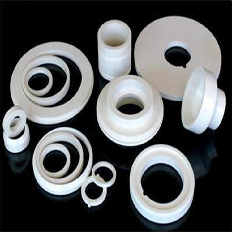
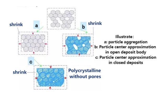
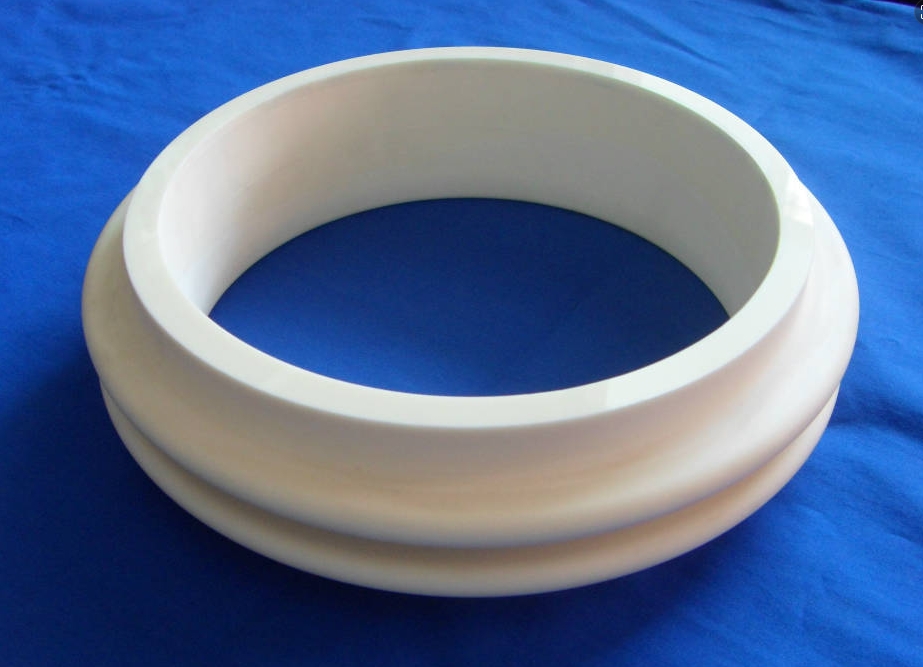
Manufacturing process of Alumina ceramics
Alumina ceramics is a ceramic material with alumina (Al2O3) as the main body for thick film integrated circuits.